
Display device and system for inspecting bonding resistance and inspecting method thereof

a display device and bonding resistance technology, applied in the field of display devices, can solve the problems of not being able to determine the bonding resistance between the display panel and the circuit board, the inspection method of the actual bonding resistance cannot be used, and the automatic optical inspection apparatus cannot determine the relative position of the pressed conductive particle number, etc., to achieve the inspection of the bonding resistance more readily, the inspection of the bonding resistance can be more accurately determined, and the acceptability of the bonding resistan

Active Publication Date: 2014-03-04
AU OPTRONICS CORP
View PDF21 Cites 0 Cited by
  • Summary
  • Abstract
  • Description
  • Claims
  • Application Information

AI Technical Summary

Benefits of technology

The patent is about a new system and method for testing the bonding resistance of integrated circuit components. The system includes testing pads and a comparator and logic circuit on the driving chip. This new system can accurately determine the resistance of the bonding and make the inspection process easier.

Problems solved by technology

The automated optical inspection apparatus, however, can only determine whether the pressed conductive particle number and the relative position between the display panel and the circuit board and between the display panel and driving chip are normal.
Alternatively speaking, the automated optical inspection apparatus is unable to inspect the actual bonding resistance between the display panel and the circuit board, and between the display panel and the driving chip.
However, not all bonding defects can be determined with this inspection method.
Hence, defective products are often not identified.
Moreover this inspection method is more complicated and time consuming.

Method used


Image

  • Display device and system for inspecting bonding resistance and inspecting method thereof
  • Display device and system for inspecting bonding resistance and inspecting method thereof
  • Display device and system for inspecting bonding resistance and inspecting method thereof

Examples


Embodiment Construction

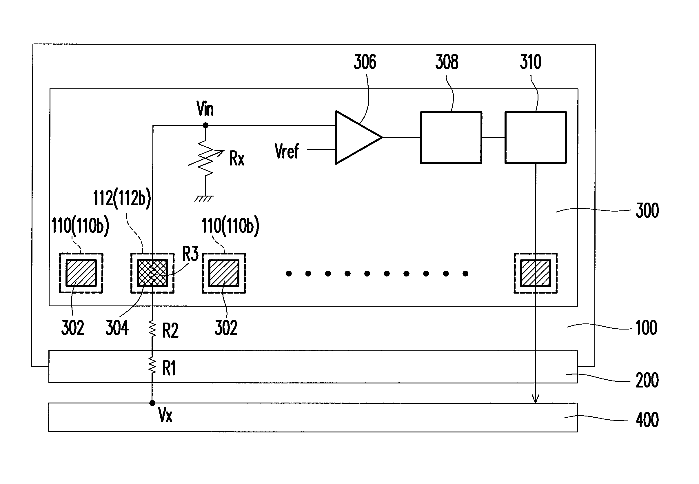
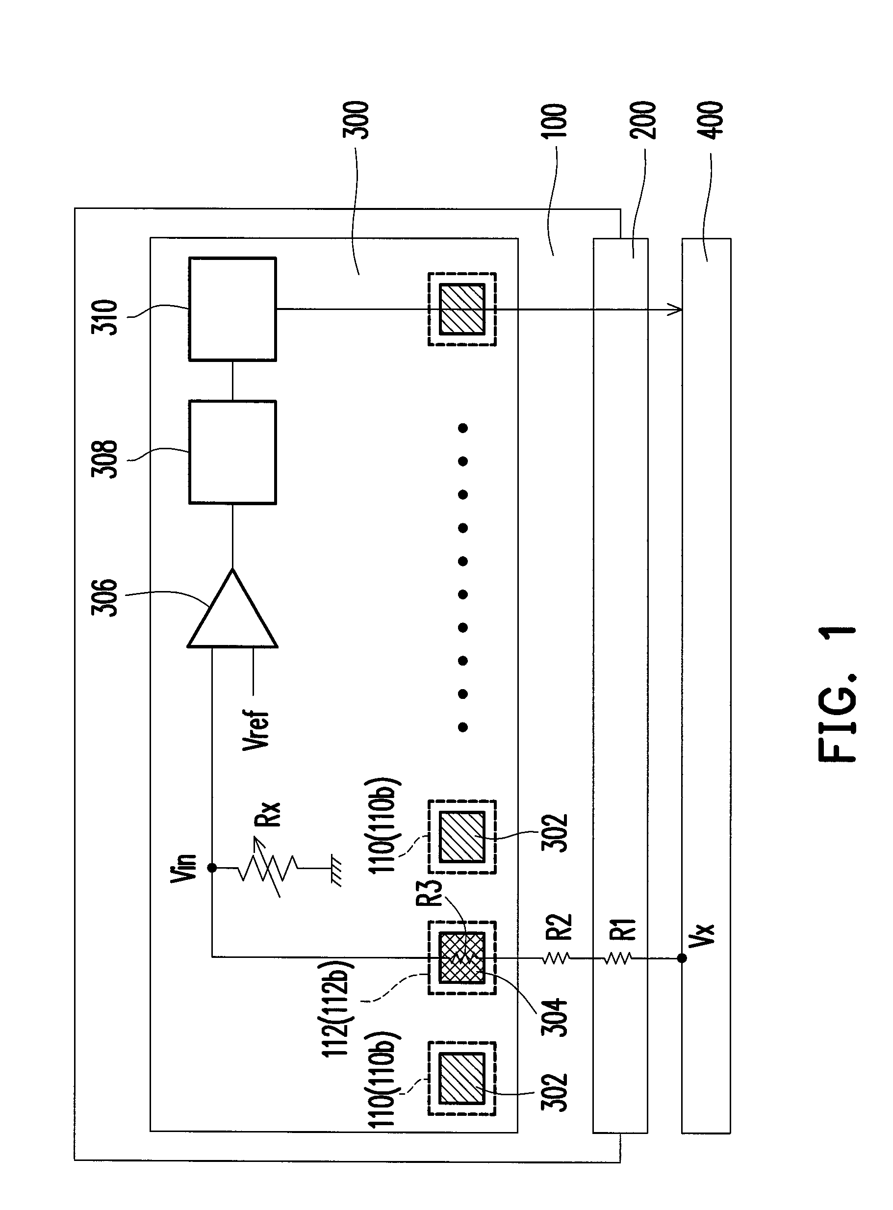
[0020]FIG. 1 is a schematic diagram of an inspection system for bonding resistance of a display device according to an exemplary embodiment of the disclosure.

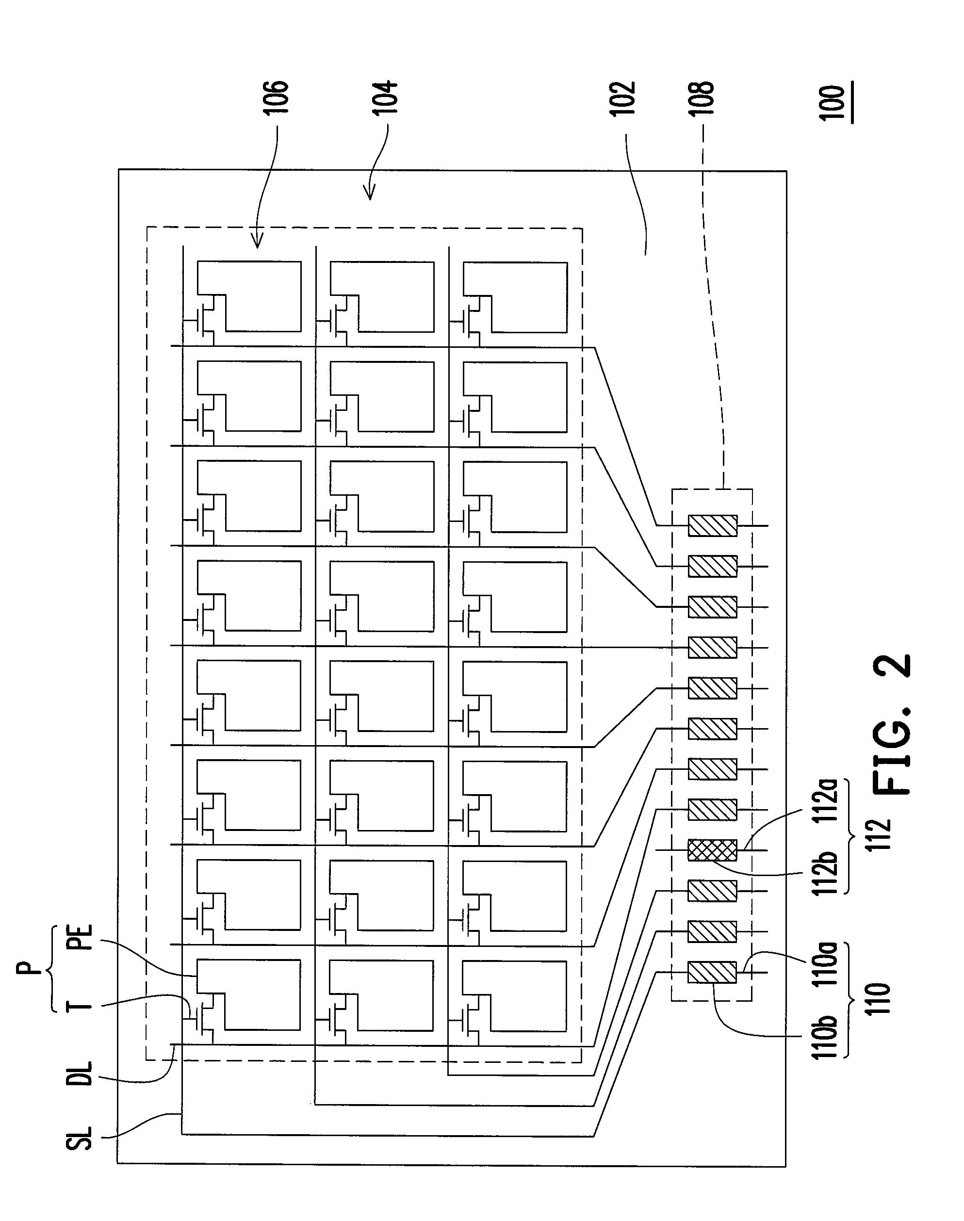
[0021]FIG. 2 is a schematic diagram of the display panel of FIG. 1. FIG. 3 is a side-view diagram of the display panel, the circuit board and the driving chip of FIG. 1. Referring concurrently to FIGS. 1, 2 and 3, the inspection system for bonding resistance of a display device according to an exemplary embodiment includes a display panel 100, at least one circuit board 200, at least one driving chip 300 and a testing board 400.

[0022]The display panel 100 includes a plurality of connecting conductive lines 110 and at least one testing conductive line 112, wherein the connecting conductive lines 110 are used for inputting or outputting various signals, and the testing conductive lines 112 are used for inputting the testing conductive signal, as shown in FIG. 2. More specifically, the display panel 100 includes a substrate 102, a...


PUM


Abstract

A system for inspecting bonding resistance of a display device includes a display panel, at least one circuit board, at least one driving chip and a testing board. The display panel includes at least one testing conductive line and connecting conductive lines. The circuit board is connected with the testing conductive line and the connecting conductive lines. The driving chip includes at least one testing pad and connecting pads, respectively electrically connected to the testing conductive line and the connecting conductive lines; at least one comparator connected to the testing pad; and at least one logic circuit connected to the comparator. The testing board is connected to the circuit board and provides a test signal to the testing pad through the circuit board and the testing conductive line. The test signal is compared with a reference signal in the comparator, and the logic circuit determines a comparing result.

Description

CROSS-REFERENCE TO RELATED APPLICATION[0001]This application claims the priority benefit of Taiwan application serial no. 99136994, filed on Oct. 28, 2010. The entirety of the above-mentioned patent application is hereby incorporated by reference herein and made a part of this specification.BACKGROUND[0002]1. Field of the Disclosure[0003]The present invention relates to a display device, and more particularly to a system for inspecting bonding resistance and an inspecting method.[0004]2. Description of Related Art[0005]Generally speaking, asides from a display panel, a display device also includes a circuit board and a driving chip for driving an image display of the display panel. After the fabrication of a display device, a series of inspection procedures is performed to ensure that the display quality of the display device conforms to standards.[0006]Currently, the method of inspecting the bonding resistance between the display panel and the circuit board, and the bonding resista...

Claims


Application Information

Patent Timeline
Patent Type & Authority Patents(United States)
IPC IPC(8): G01R27/08
CPCG02F1/1345G09G3/006G01R27/08G02F1/1309
Inventor CHEN, CHIH-MINGLIN, NENG-YI
Owner AU OPTRONICS CORP
Learn More