Electronic device

a technology of electronic devices and keys, applied in the field of electronic devices, can solve the problems of increased production and assembly costs of additional light sources for keys, difficulty in the operation of keys, and increased power consumption, and achieve the effects of reducing production and assembly costs, reducing luminance differences, and clearly distinguishing keys

Inactive Publication Date: 2014-04-01
COMPAL ELECTRONICS INC
View PDF7 Cites 3 Cited by
  • Summary
  • Abstract
  • Description
  • Claims
  • Application Information

AI Technical Summary

Benefits of technology

[0018]In light of the above, when the display module of the electronic device of the invention emits light onto the keyboard module, the light guiding portion on each key directs the light towards a specific direction, and the light scattering portion on each key scatters the light in other directions, thereby creating a difference in luminance between the light guiding portion and the light scattering portion. When a user operates the electronic device in a dark environment, the difference in luminance between the light guiding portion and the light scattering portion assists the user in clearly distinguishing the keys. Since the keys use the light emitted from the display module to induce the difference in luminance between the light guiding portion and light scattering portion and does not require additional light sources corresponding to the keys to be installed, the production and assembly costs are reduced.

Problems solved by technology

When the users try to operate the electronic device in a dark environment, the low lighting causes difficulty in the operation of the keys.
However, additional light sources for keys incur additional costs in production and assembly, consume more power and are consequently less environmental friendly.
In consequence, a simpler design that allows the users to conveniently operate the keys in dark environments is an important issue in the field of designs of current electronic devices.

Method used


Image

  • Electronic device
  • Electronic device
  • Electronic device

Examples


Embodiment Construction

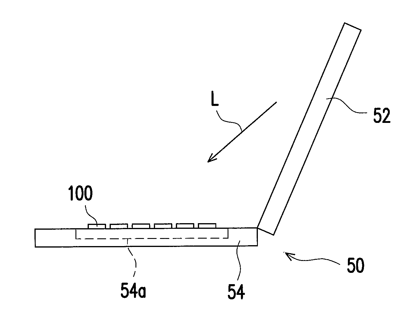
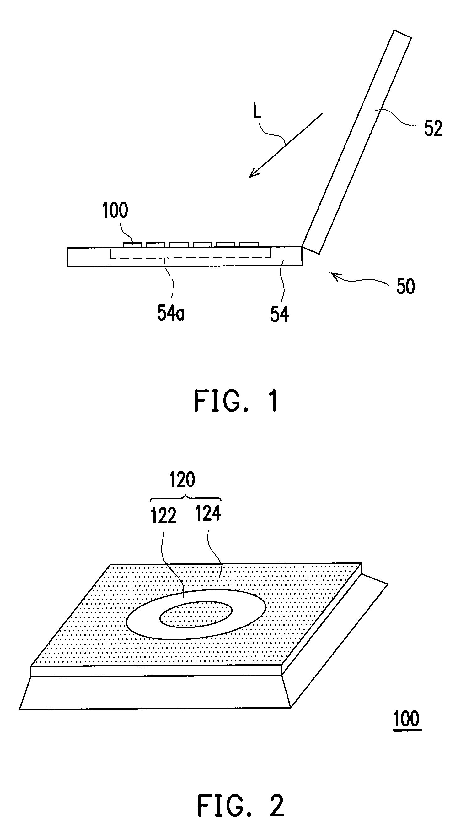
[0028]FIG. 1 is a schematic view of an electronic device of an embodiment of the invention. Referring to FIG. 1, an electronic device 50 of the present embodiment is, for example, a notebook computer and includes a display module 52 and a base 54. The display module 52 (shown as open) is pivoted on the base 54 and is suited to be opened and closed on the base 54. A keyboard module 54a is disposed on the base 54 and has a plurality of keys 100 for a user to press.

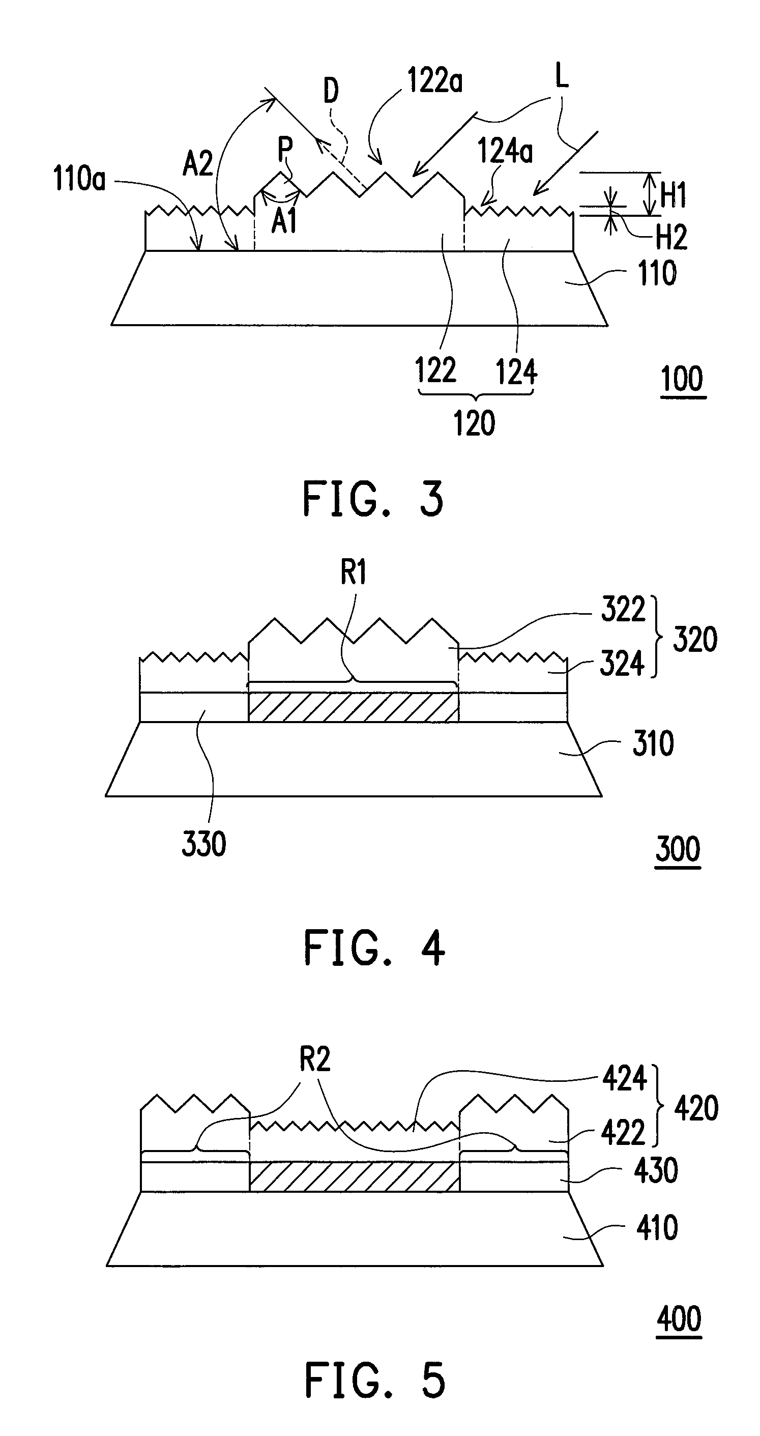
[0029]FIG. 2 is a three dimensional view of a key in FIG. 1. FIG. 3 is a cross-sectional view of the key in FIG. 2. Referring to FIGS. 2 and 3, the key 100 includes a main body 110 and an imprinted structure 120. The main body 110 is disposed on the base 54 illustrated in FIG. 1 and has a top surface 110a. The imprinted structure 120 is installed on the top surface 110a of the main body 110 and includes a light guiding portion 122 and a light scattering portion 124.

[0030]When the display module 52 in FIG. 1 displays a screen...


PUM


Abstract

An electronic device includes a display module, a base and a keyboard module. The display module is pivoted on the base. The keyboard module is disposed on the base. The keyboard module has a plurality of keys. Each of the keys includes a main body and an imprinted structure. The main body has a top surface. The imprinted structure is disposed on the top surface of the main body and includes a light guiding portion and a light scattering portion. A light emitted by the display module illuminates the keyboard module. The light is guided towards a specific direction when the light passes through the light guiding portion, and the light is scattered in other directions when the light passes through the light scattering portion.

Description

CROSS-REFERENCE TO RELATED APPLICATION[0001]This application claims the priority benefit of Taiwan application serial no. 101112264, filed on Apr. 6, 2012. The entirety of the above-mentioned patent application is hereby incorporated by reference herein and made a part of this specification.BACKGROUND OF THE INVENTION[0002]1. Field of the Invention[0003]The invention relates to an electronic device, and more particularly to an electronic device having a keyboard module.[0004]2. Description of Related Art[0005]With the flourishing advancement of technology, the types and functions of electronic devices are becoming ever more diverse. Regardless of the type of the electronic device, for users, the traditional and common method of using the electronic device is to press physical keys on the device to perform various operations.[0006]When the users try to operate the electronic device in a dark environment, the low lighting causes difficulty in the operation of the keys. For this reason...

Claims


Application Information

Patent Timeline
Patent Type & Authority Patents(United States)
IPC IPC(8): F21V7/04
CPCH01H2231/002H01H2219/028H01H2229/008G06F1/18H01H13/83H01H2219/056G06F3/0202H01H2219/062
Inventor CHUANG, WAN-LICHANG, CHIEN-MINYU, LI-JUNGTSAI, MEI-HSIUNGCHANG, YUNG-CHINGCHIU, JU-CHEN
Owner COMPAL ELECTRONICS INC
Why Eureka
Try Eureka