
Eureka
For R&D, Eureka makes reading and utilizing patents & technical documents easy.
Eureka AIR
Designed for self-driven R&D workflows. Generate viable solutions, solve complex R&D challenges, empower your innovation with AI.

Eureka Materials
Designed for material experts only. Revolutionize your material R&D, from search, analyze, to developing new materials.

TechResearch
Generate reliable direction feasibility study reports for your R&D in just a few steps.

TechSeek
Discover and master advanced knowledge NOW. Basics, ideas, possibilities, all at once.

TechMind
As an expert in R&D Theories, TechMind can generates customized viable solutions instantly.

TechRisk
Analyze your overall solution with one click, know your potential R&D risks in advance.

TechMonitor
Get weekly tech updates, stay abreast of the latest tech innovations and key insights.
Method of making a low-Rdson vertical power MOSFET device
- Summary
- Abstract
- Description
- Claims
- Application Information
AI Technical Summary
Problems solved by technology
Method used
Image

Examples
Example
Embodiment I
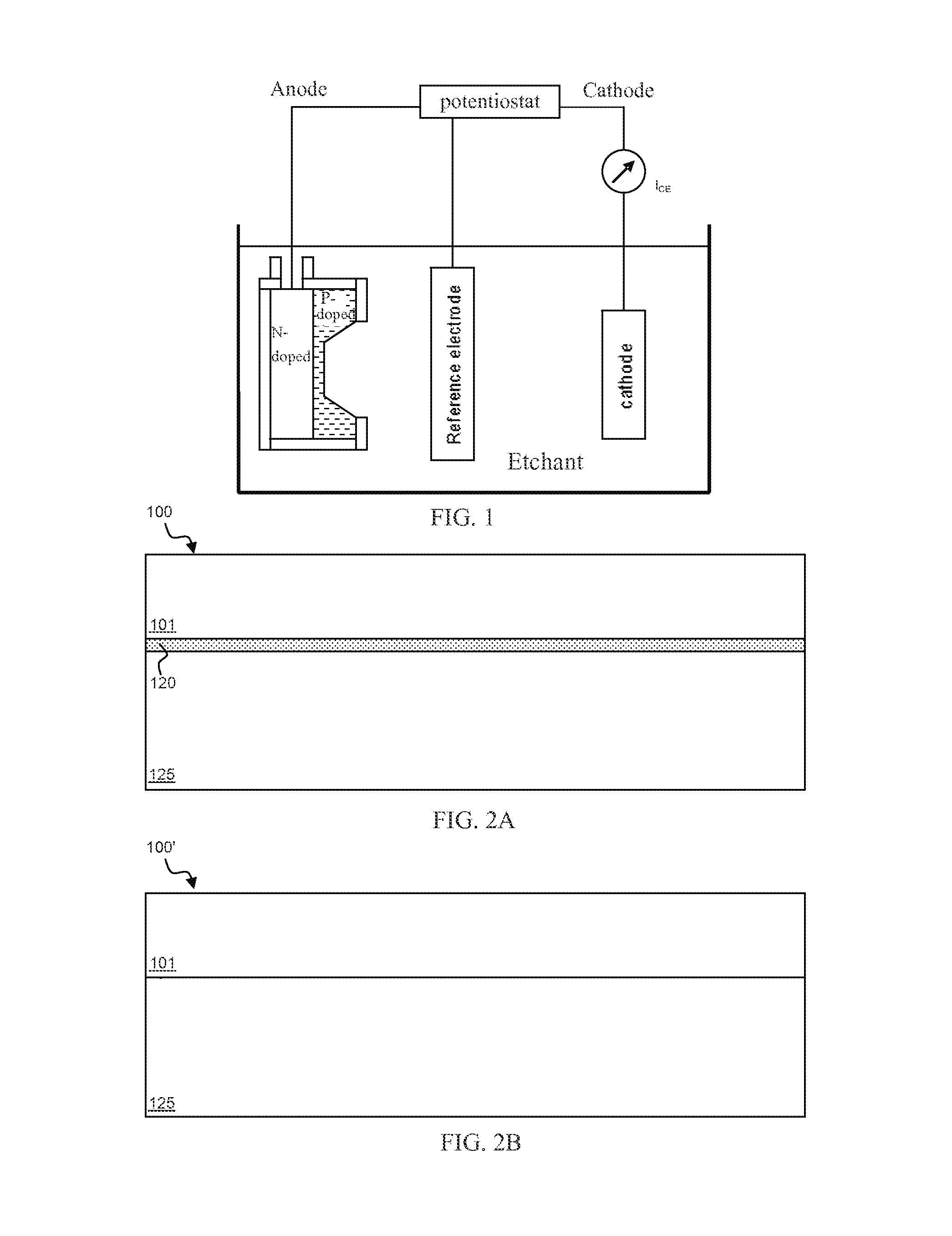
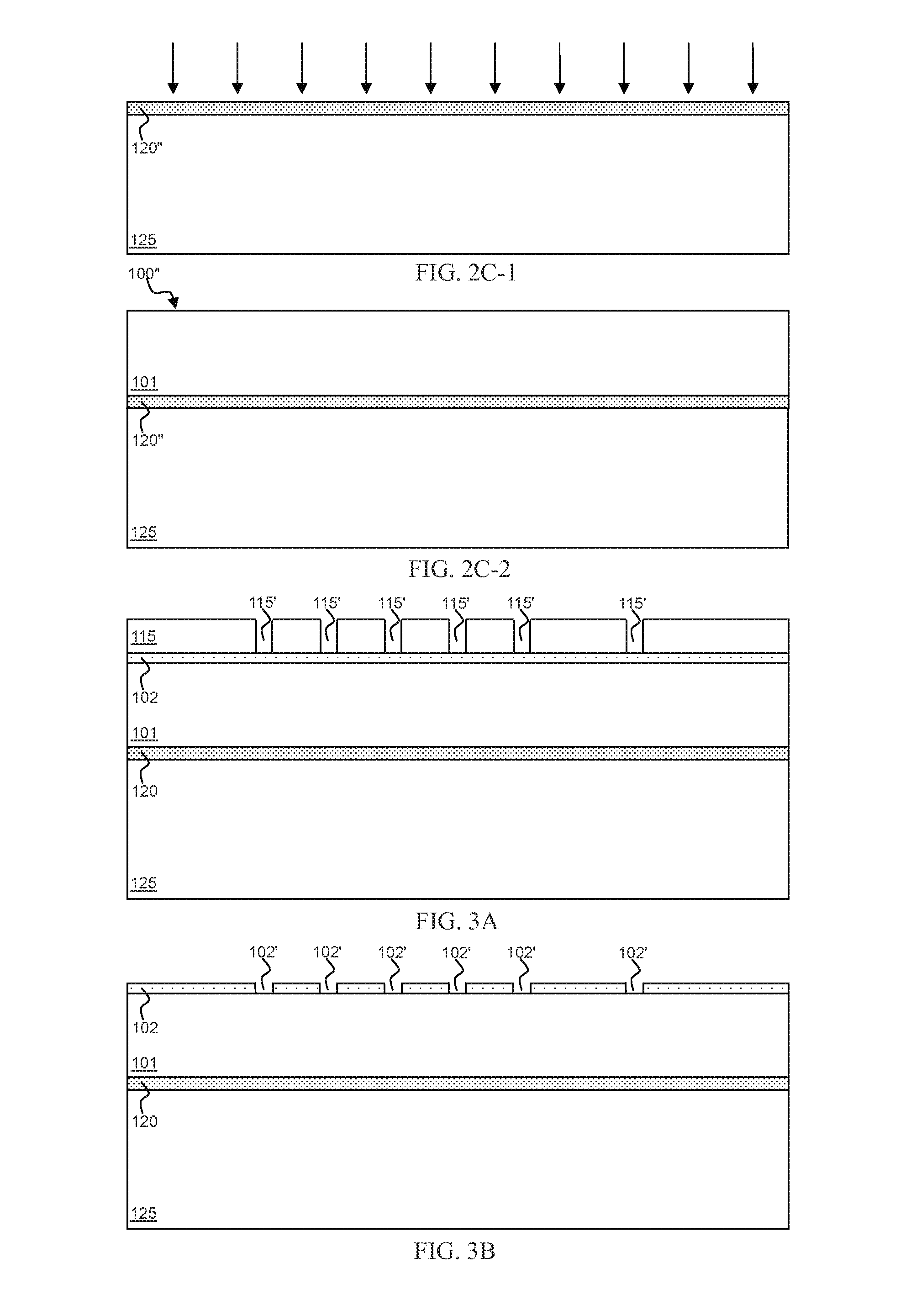
[0022]As shown in FIG. 2A, an etching barrier layer 120 is arranged between a substrate 125 and an epitaxial layer 101 in a wafer 100, which is usually called a SOI (silicon on insulator) wafer. However, the epitaxial layer 101 is directly grown on the substrate 125 in wafer 100′ as shown in FIG. 2B. Dopants may be implanted on the top surface of the substrate 125 first to form a buried heavily doped layer 120″ in wafer 100″ as shown in FIG. 2C-1 and FIG. 2C-2, for example, a P+ buried heavily doped layer 120″ maybe implanted at the top surface of lightly doped P− substrate 125, then a lightly doped P− epitaxial layer 101 is grown on the substrate 125. Thus, the buried heavily doped layer 120″ is formed between the substrate 125 and the epitaxial layer 101.
[0023]In FIG. 3A, an oxide layer 102 (such as a LTO-low temperature oxide) is formed covering on epitaxial layer 101, then a photoresist layer 115, which is patterned with a plurality of openings 115′, is coated on the...
Example
Embodiment II
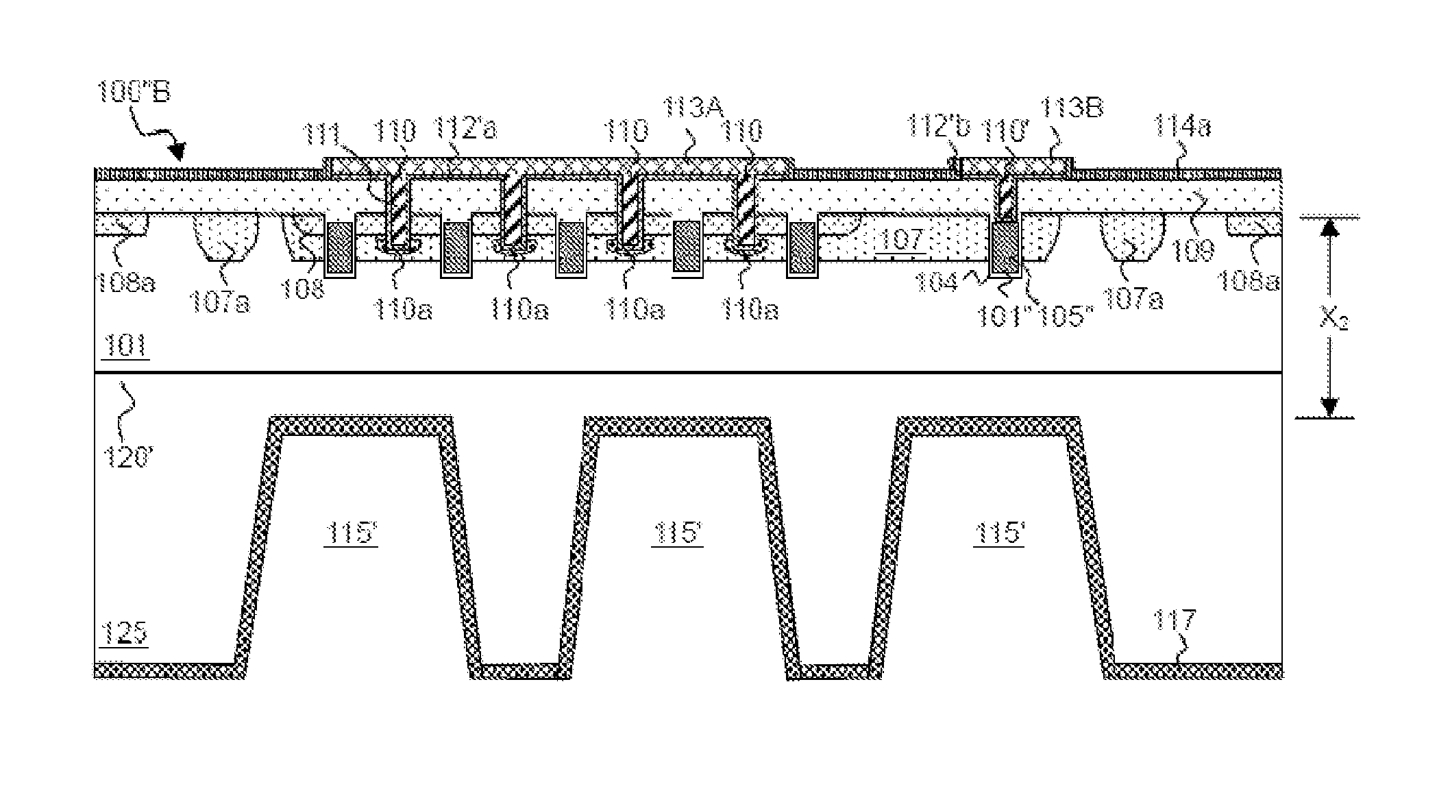
[0026]As shown in the FIG. 2B and the FIGS. 4A-4D, the epitaxial layer 101 is directly grown on the substrate 125 in a wafer 100′; both the substrate and the epitaxial layer are lightly doped. If the prepared vertical MOSFET unit is implemented in the wafer 100′, then the procedures of preparing the vertical MOSFET unit in the epitaxial layer 101 are not different from that in the embodiment I; therefore, the same vertical MOSFET units are formed in the epitaxial layer 101 supported by the substrate 125. However, in this embodiment the doping conductivity types of the substrate 125 and the epitaxial layer 101 are opposite. The purpose is to use the PN junction at the interface of the substrate 125 and the epitaxial layer 101 as an etching barrier layer when the substrate 125 is etched. As shown in the FIG. 4A, the bottom passivation layer 114b is deposited on the bottom surface of the substrate 125. One or more openings 114b′ (for the purpose of conciseness, only one op...
PUM
 Abstract
Description
Claims
Application Information
 - R&D Engineer
- R&D Manager
- IP Professional
- Industry Leading Data Capabilities
- Powerful AI technology
- Patent DNA Extraction
Browse by: Latest US Patents, China's latest patents, Technical Efficacy Thesaurus, Application Domain, Technology Topic, Popular Technical Reports.
© 2024 PatSnap. All rights reserved.Legal|Privacy policy|Modern Slavery Act Transparency Statement|Sitemap|About US| Contact US: help@patsnap.com