Semiconductor device having stacked structure including through-silicon-vias and method of testing the same

a technology of semiconductors and structures, applied in semiconductor/solid-state device testing/measurement, instruments, basic electric elements, etc., can solve problems such as difficulty in accurately testing tsvs and defects of tsvs

Inactive Publication Date: 2012-06-07
SAMSUNG ELECTRONICS CO LTD
View PDF3 Cites 132 Cited by
  • Summary
  • Abstract
  • Description
  • Claims
  • Application Information

AI Technical Summary

Benefits of technology

[0009]The present general inventive concept provides a semiconductor device having a circuit capable of measuring a resistance-capacitanc

Problems solved by technology

However, when the multiple chips are stacked three-dimensionally by using the TSVs, s

Method used


Image

  • Semiconductor device having stacked structure including through-silicon-vias and method of testing the same
  • Semiconductor device having stacked structure including through-silicon-vias and method of testing the same
  • Semiconductor device having stacked structure including through-silicon-vias and method of testing the same

Examples


Embodiment Construction

[0042]Reference will now be made in detail to the embodiments of the present general inventive concept, examples of which are illustrated in the accompanying drawings, wherein like reference numerals refer to the like elements throughout. The embodiments are described below in order to explain the present general inventive concept while referring to the figures.

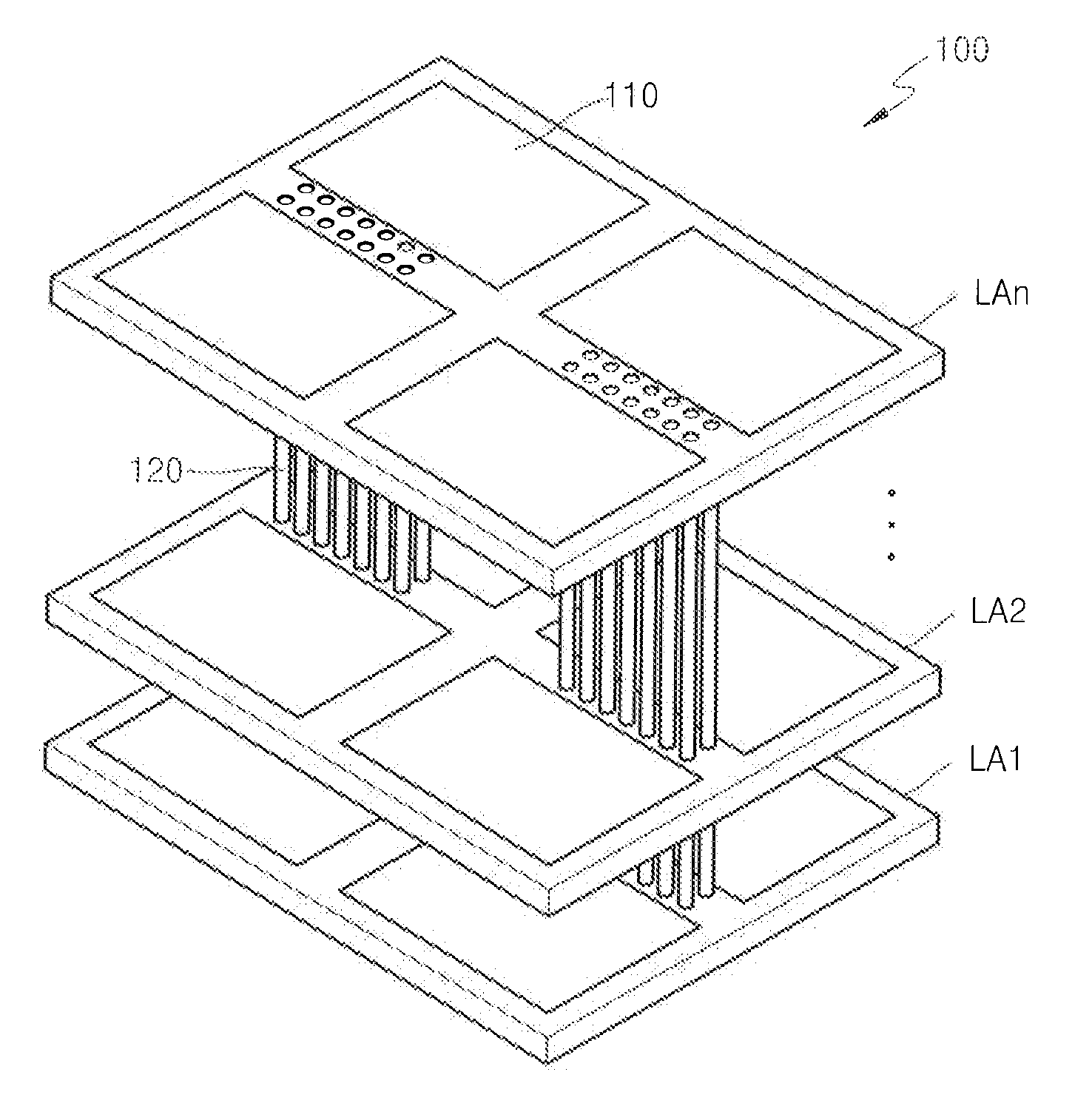
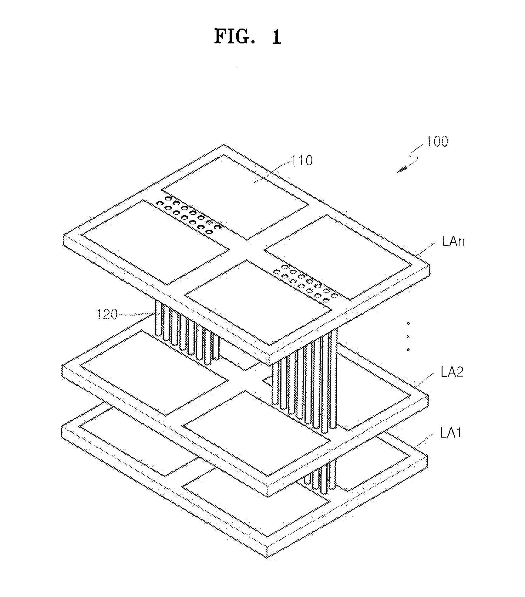
[0043]FIG. 1 is a schematic diagram of a semiconductor device having a stacked structure including a plurality of semiconductor layers. Referring to FIG. 1, a semiconductor device 100 includes a plurality of layers LA1 through LAn in a stacked structure, which are interconnected by through-silicon-vias (TSVs) 120. Each of the layers LA1 through LAn includes a plurality of circuit blocks 110 to implement functions of the semiconductor device 100. The semiconductor device 100 may be a semiconductor memory device including memory cells, and in this case, each of the layers LA1 through LAn may be referred to as a cell layer and t...


PUM


Abstract

A semiconductor device having a stacked structure including through-silicon-vias (TSVs) and a method of testing the semiconductor device. The semiconductor device includes a first semiconductor layer, one or more second semiconductor layers stacked on the first semiconductor layer, and a plurality of input through-silicon-vias (TSVs) to transmit signals from a plurality of input pads, respectively. In a test mode, a test signal from the plurality of input pads is transmitted through at least two test paths, and the test signal transmitted through each of the test paths is output as a test result with respect to each of the plurality of input TSVs through an output pad.

Description

CROSS-REFERENCE TO RELATED APPLICATIONS[0001]This application claims the benefit of priority under 35 U.S.C.§119 to Korean Patent Application No. 10-2010-0123476, filed on Dec. 6, 2010, in the Korean Intellectual Property Office, the disclosure of which is incorporated herein in its entirety by reference.BACKGROUND OF THE INVENTION[0002]1. Field of the Invention[0003]The present general inventive concept generally relates to a semiconductor device having a stacked structure including through-silicon-vias (TSVs) and a method to test a connection state of the TSVs of the semiconductor device,[0004]2. Description of the Related Art[0005]A multi-chip package (MCP) is a package chip having multiple chips. In an MCP, necessary memories may be combined in applicable products and space efficiency of mobile devices such as mobile phones may be significantly improved.[0006]In a three-dimensional (3D) stacking scheme, which is one method for manufacturing the MCP, multiple chips are stacked in...

Claims


Application Information

Patent Timeline
IPC IPC(8): H01L23/00
CPCG01R31/318513H01L22/14H01L25/0657H01L2225/06513H01L2225/06544H01L2924/0002H01L2225/06596H01L2924/00
Inventor KANG, UK-SONG
Owner SAMSUNG ELECTRONICS CO LTD
Why Eureka
Try Eureka