

Semiconductor device, manufacturing method thereof, and electronic apparatus
a technology of semiconductor devices and semiconductors, applied in the direction of semiconductor/solid-state device details, radiation control devices, television systems, etc., can solve the problems of difficult to practically realize the above idea, unfavorable increase in cost, and limited material for connecting conductors, etc., to achieve high performance, high efficiency, and the effect of superior mass productivity
- Summary
- Abstract
- Description
- Claims
- Application Information
AI Technical Summary
Benefits of technology
Problems solved by technology
Method used
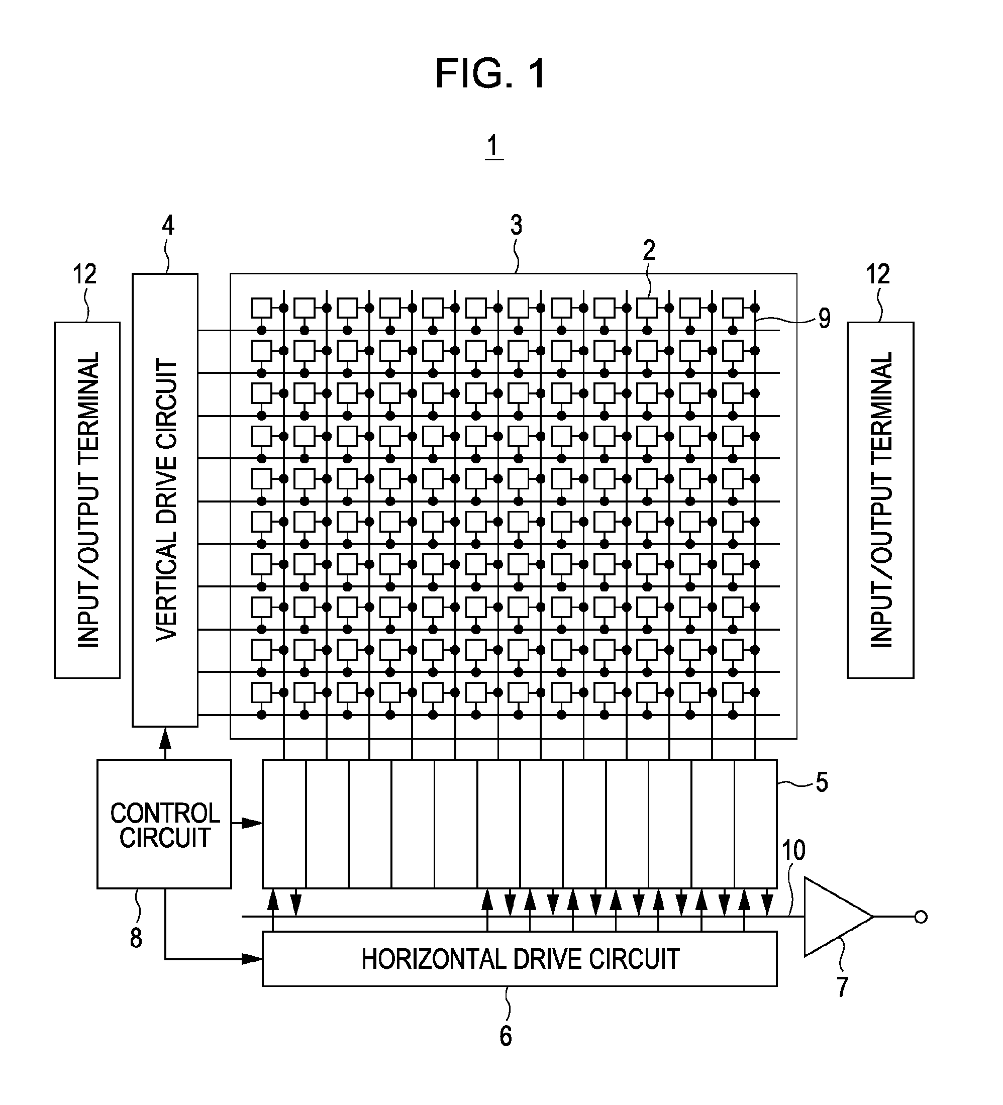
Image

Examples
first embodiment
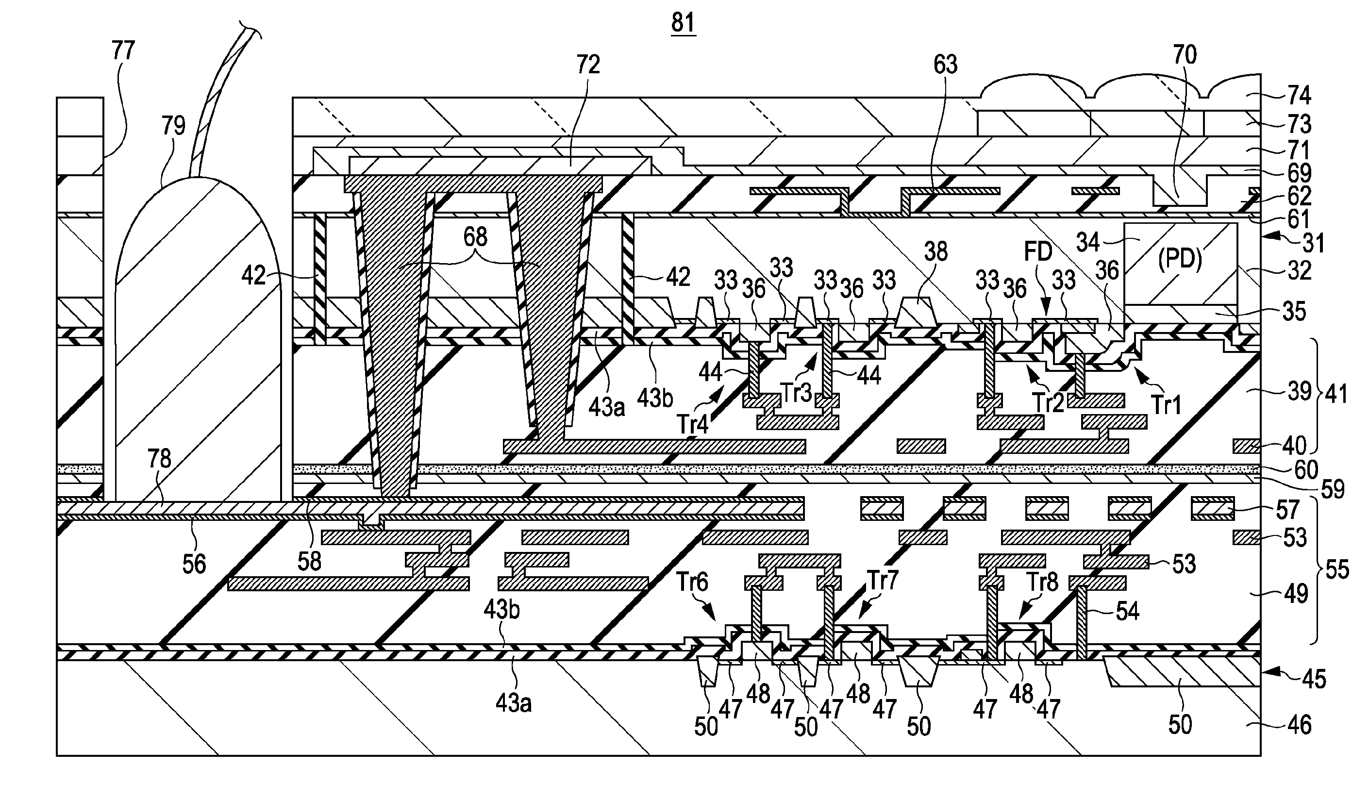
[0144]In the solid-state image pickup device although the case in which the bonding wire 79 is connected to the electrode pad portion 78 is described by way of example, the electrode pad portion 78 and the external wire may be connected to each other by using a solder bump. Depending on a user's request, the bonding wire or the solder bump may be selected.
[0145]In the first embodiment, inspection of the solid-state image pickup devices in a semiconductor wafer state is performed using the electrode pad portions 78. In addition, two inspections, that is, an inspection in a wafer state and an inspection in a final module state obtained by chip division, are performed.
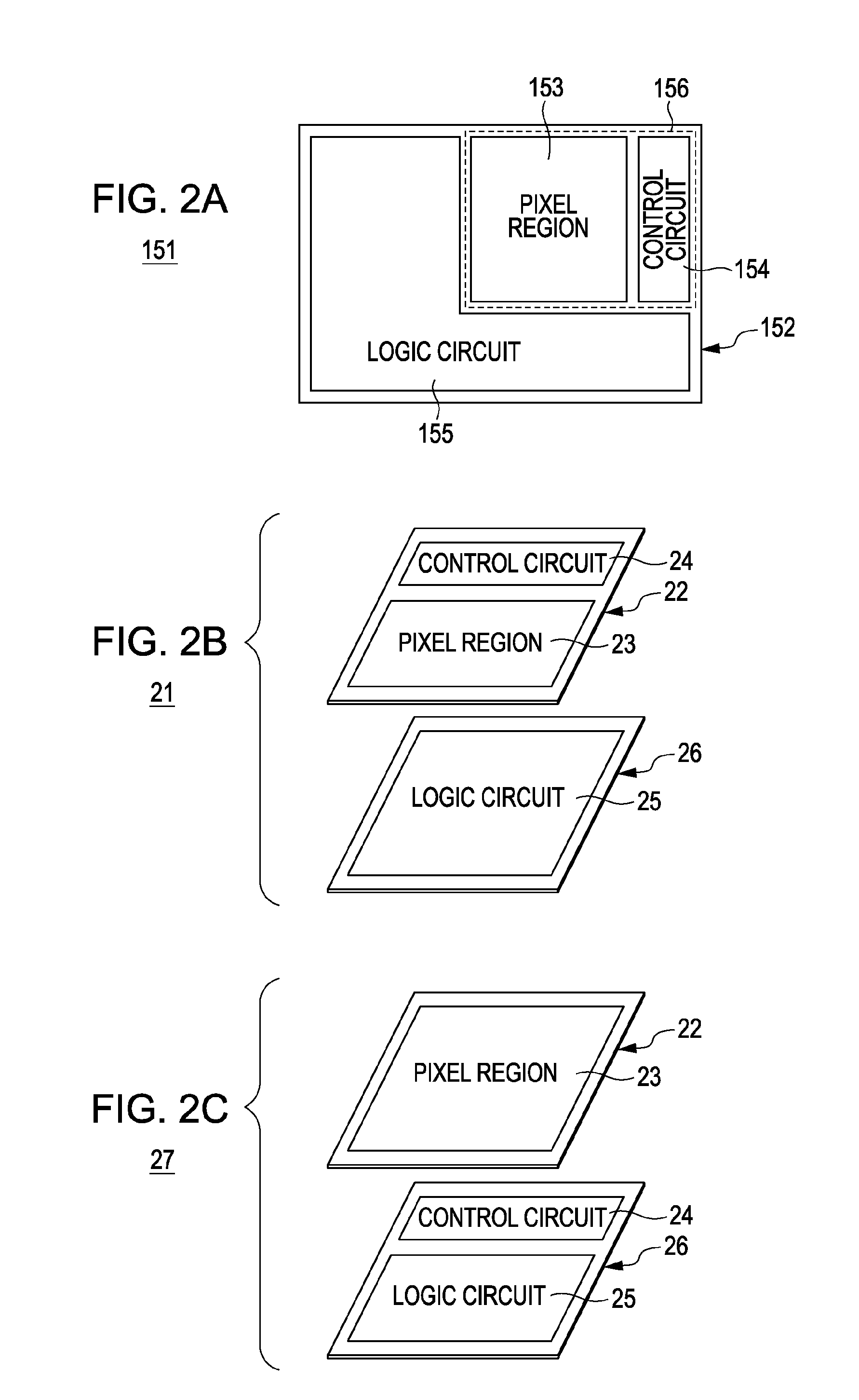
[0146]In the solid-state image pickup device according to the first embodiment and the manufacturing method thereof, the pixel region 23 and the control circuit 24 are formed on a chip portion of the first semiconductor substrate 31, and the logic circuit 25 performing signal processing is formed on a chip portion of the...
second embodiment
[0153]FIG. 21 is a schematic structural view showing a solid-state image pickup device according to the present invention. As in FIG. 3, FIG. 21 is a schematic structural view showing an area including a region in which a pad portion is formed. A solid-state image pickup device 82 of this embodiment shows one structural example in which since an inter-substrate wire 80 is formed from one connection hole, a pixel region and a control circuit at a first semiconductor substrate 31 side and a logic circuit at a second semiconductor substrate 45 side are electrically connected to each other. In FIG. 21, elements corresponding to those shown in FIG. 3 are designated by the same reference numerals and descriptions thereof are omitted.
[0154]In this embodiment, the inter-substrate wire 80 electrically connecting between the first semiconductor substrate 31 and the second semiconductor substrate 45 penetrates the first semiconductor substrate 31 from a rear surface side thereof and reaches a ...
third embodiment
[0159]With reference to FIG. 22 and FIGS. 23 to 28, a semiconductor device according to the present invention and a manufacturing method thereof will be described. A semiconductor device 140 of this embodiment is a semiconductor device including a first semiconductor substrate 101 on which a first semiconductor integrated circuit is formed and a second semiconductor substrate 102 on which a second semiconductor integrated circuit is formed, the first and the second semiconductor substrates being laminated to each other. In FIG. 22, elements corresponding to those in FIG. 3 are designated by the same reference numerals and descriptions thereof are omitted.
[0160]In the third embodiment, first, as shown in FIG. 23, on a region to be formed into each chip portion of the first semiconductor substrate (semiconductor wafer) 101, a semi-finished first semiconductor integrated circuit, that is, a logic circuit in this embodiment, is formed. That is, on a region to be formed into each chip po...
PUM
 Abstract
Description
Claims
Application Information