Resist pattern thickening material, resist pattern and process for forming the same, and semiconductor device and process for manufacturing the same

a technology of resist pattern and thickening material, which is applied in the direction of photosensitive materials, auxiliary/base layers of photosensitive materials, instruments, etc., can solve the problems of inability to efficiently thicken resist pattern, inability to use arf excimer laser as exposure light, etc., and achieve efficient thickening of resist pattern

Inactive Publication Date: 2006-04-06
FUJITSU LTD
View PDF19 Cites 39 Cited by
  • Summary
  • Abstract
  • Description
  • Claims
  • Application Information

AI Technical Summary

Benefits of technology

[0010] An object of the present invention is to provide a resist pattern thickening material which, when applied on a resist pattern, can efficiently thicken the resist pattern, and which is suited to formation of a fine space pattern, exceeding the exposure limits of light sources of existing exposure devices.

Problems solved by technology
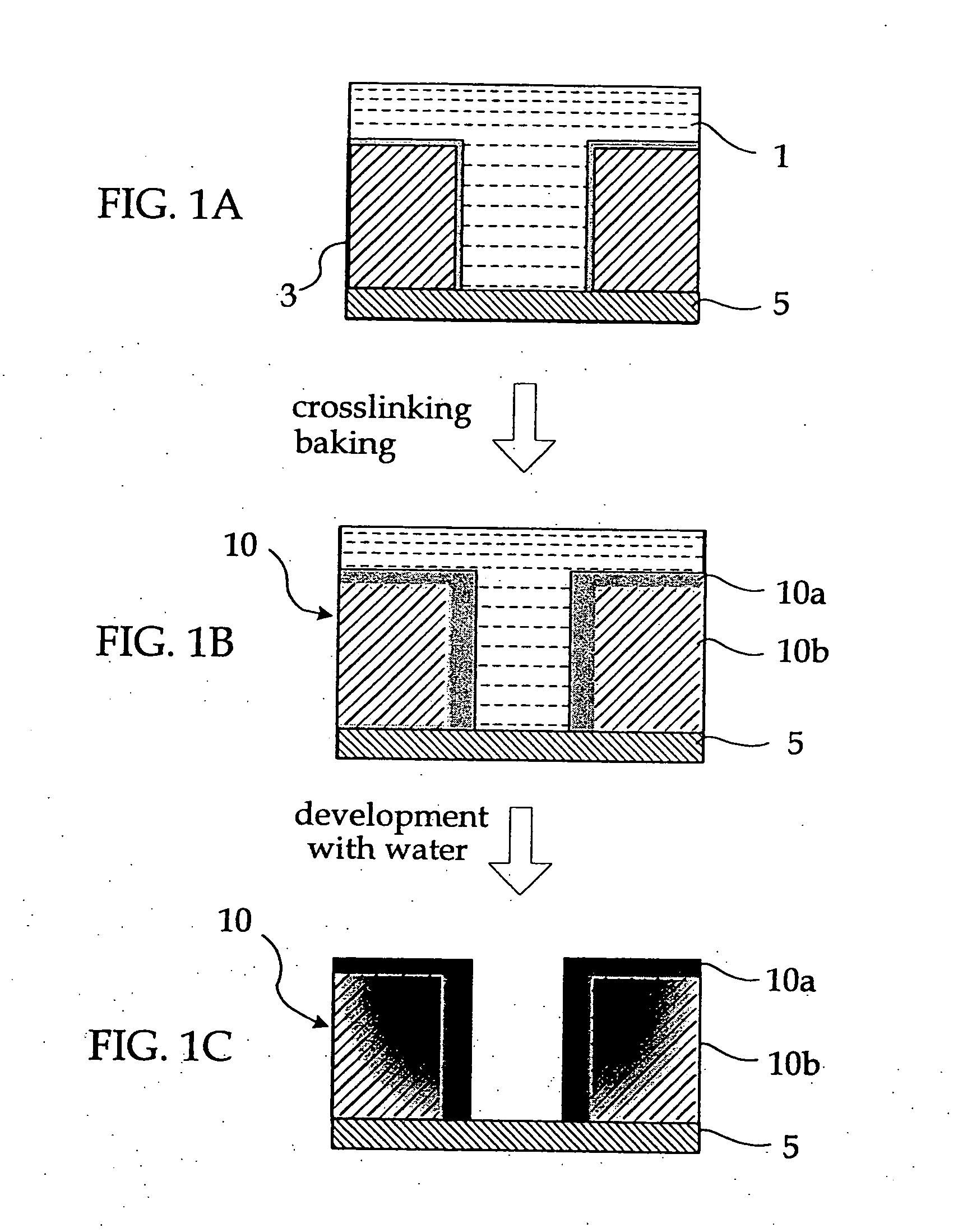
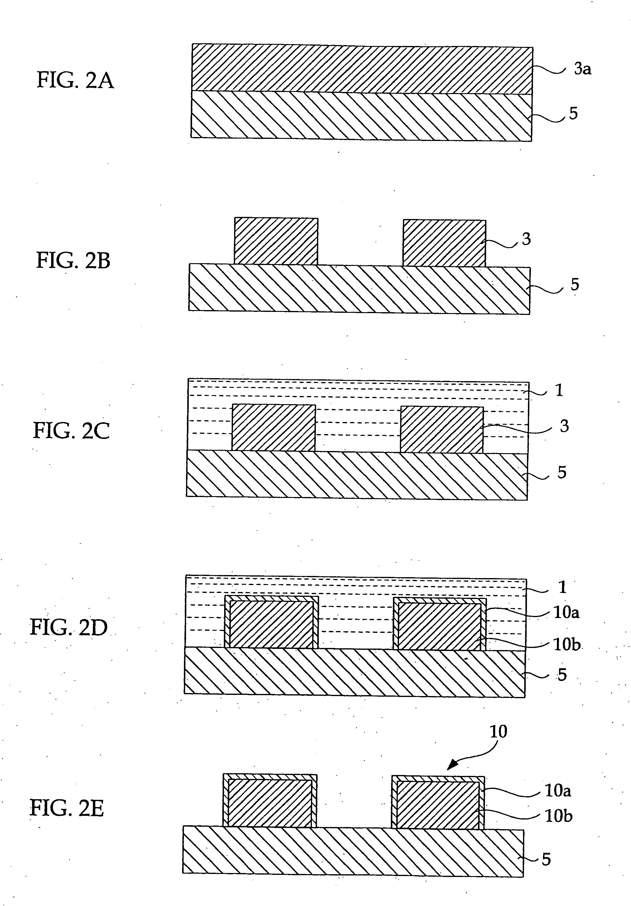
However, in the above-described technique, it is not possible to use ArF excimer laser as the exposure light, instead of KrF excimer laser.
However, using an ArF resist as the resist in the above-described technique, a problem arises in that the resist pattern cannot be thickened efficiently.
Therefore, the current situation is that there has not yet been developed techniques such as materials, methods and the like which, after forming a resist pattern by using ArF excimer laser as well as KrF excimer laser as the exposure light, can form an applied film on the resist pattern and thicken the resist pattern.

Method used


Image

  • Resist pattern thickening material, resist pattern and process for forming the same, and semiconductor device and process for manufacturing the same
  • Resist pattern thickening material, resist pattern and process for forming the same, and semiconductor device and process for manufacturing the same
  • Resist pattern thickening material, resist pattern and process for forming the same, and semiconductor device and process for manufacturing the same

Examples


example 1

-Preparation of Resist Pattern Thickening Material-

[0143] Resist pattern thickening materials A through O of the present invention having the compositions shown in Table 1 were prepared. Note that, in Table 1, the unit of the values in parentheses is parts by mass. In the “resin” column, “KW-3” is a polyvinyl acetal resin (manufactured by Sekisui Chemical Co., Ltd.). In the “crosslinking agent” column, “uril” is tetramethoxymethylglycol uril, and “urea” is N,N′-dimethoxymethyldimethoxyethylene urea. In the “surfactant” column, “SO-135” is a non-ionic surfactant (a secondary alcohol ethoxylate surfactant manufactured by Asahi Denka Co., Ltd.), “NP-675” is a non-ionic surfactant (a nonylphenol ethoxylate surfactant manufactured by Asahi Denka Co., Ltd.), “SP-12” is a non-ionic surfactant (a special phenol ethoxylate surfactant manufactured by Asahi Denka Co., Ltd.), “T-81” is a non-ionic surfactant (a sorbitan ester surfactant manufactured by Asahi Denka Co., Ltd.), “LB-53B” is a no...

example 2

-Flash Memory and Process for Manufacturing the Same-

[0155] Example 2 is an example of the semiconductor device and a process for manufacturing the same of the present invention using the resist pattern thickening material of the present invention. Note that, in Example 2, resist films (resist patterns) 26, 27, 29, 32, and 34 which will be described hereinafter are resist films which have been thickened by the same method as in Examples 1 by using the resist pattern thickening material of the present invention.

[0156]FIGS. 3A and 3B are top views (plan views) of a FLASH EPROM which is called a FLOTOX type or an ETOX type. Note that FIGS. 4A through 4C, FIGS. 5 D through 5F, and FIGS. 6G through 6I are cross-sectional schematic views for explaining an example of a process for manufacturing the FLASH EPROM. In FIGS. 4A through 6I, the illustrations at the left sides are the memory cell portion (a first element region), and are schematic diagrams of the cross-section (the A direction...

example 3

-Manufacturing of Recording Head-

[0180] Example 3 relates to the manufacturing of a recording head as an applied example of the resist pattern of the present invention using the resist pattern thickening material of the present invention. Note that, in Example 3, resist patterns 102 and 126 which will be described hereinafter are resist patterns which have been thickened by the same method as in Example 1 by using the resist pattern thickening material of the present invention.

[0181]FIGS. 9A through 9D are process diagrams for explaining the manufacturing of the recording head.

[0182] First, as shown in FIG. 9A, a resist film was formed to a thickness of 6 μm on an interlayer insulating film 100. Exposure and developing were carried out, so as to form the resist pattern 102 having an opening pattern for formation of a spiral, thin film magnetic coil.

[0183] Next, as shown in FIG. 9B, a plating underlying layer 106 was formed by vapor deposition on the interlayer insulating layer ...


PUM

PropertyMeasurementUnit
wavelengthaaaaaaaaaa
boiling pointaaaaaaaaaa

Abstract

The present invention provides a resist pattern thickening material and the like which can thicken a resist pattern and form a fine space pattern. The resist pattern thickening material contains: a resin; a crosslinking agent; and at least one type selected from cationic surfactants, amphoteric surfactants, and non-ionic surfactants selected from alkoxylate surfactants, fatty acid ester surfactants, amide surfactants, alcohol surfactants, and ethylene diamine surfactants. In a process for forming a resist pattern of the present invention, after a resist pattern is formed, the thickening material is applied onto a surface of the pattern. A process for manufacturing a semiconductor device of the present invention includes: after forming a resist pattern on an underlying layer, applying the thickening material on a surface of the pattern so as to thicken the pattern; and a step of patterning the underlying layer by etching by using the pattern.

Description

CROSS-REFERENCE TO RELATED APPLICATIONS [0001] This application is based upon and claims the benefit of priority from the prior Japanese Patent Application No. 2002-217213, filed on Jul. 25, 2002, the entire contents of which are incorporated herein by reference. This application is a continuation application of prior application Ser. No. 10 / 623,679 filed on Jul. 22, 2003.BACKGROUND OF THE INVENTION [0002] 1. Field of the Invention [0003] The present invention relates to a resist pattern thickening material which is applied onto a resist pattern and thickens the resist pattern, and which can form a fine space pattern exceeding exposure limits of light sources of existing exposure devices (“space pattern” is hereby defined as a hole, trench, recess, or any other empty space that is formed by a developed (removed) resist). The present invention also relates to a resist pattern, a process for forming the resist pattern, a semiconductor device, and a process for manufacturing the semico...

Claims


Application Information

Patent Timeline
Patent Type & Authority Applications(United States)
IPC IPC(8): G03C1/76G03F7/00G03F7/40G11B5/17G11B5/31H01L21/02H01L21/027H01L21/3065H01L21/8242H01L21/8247H01L27/105
CPCG03F7/0035G03F7/40G11B5/17G11B5/313G11B5/3163H01L28/10H01L27/10844H01L27/10894H01L27/11526H01L27/11541H01L27/11543H01L27/105H10B12/01H10B12/09H10B41/47H10B41/40H10B41/48G03F7/0045H01L21/027
Inventor NOZAKI, KOJIKOZAWA, MIWA
Owner FUJITSU LTD
Why Eureka
Try Eureka