Method for manufacturing semiconductor device

a manufacturing method and semiconductor technology, applied in semiconductor devices, semiconductor/solid-state device details, electrical devices, etc., can solve the problems of limiting the use of larger srafs, poor device quality, and burden on mask manufacture and defect inspection, so as to achieve high dimension precision, high quality, and efficient manufacturing

Active Publication Date: 2012-01-10
FUJITSU SEMICON LTD
View PDF16 Cites 1 Cited by
  • Summary
  • Abstract
  • Description
  • Claims
  • Application Information

AI Technical Summary

Benefits of technology

[0017]The method of the present invention for manufacturing a semiconductor device includes: forming a resist pattern on a work surface; and applying over a surface of the resist pattern a resist pattern thickening material containing at least a resin and a compound represented by the following general formula (1) to thereby thicken the resist pattern to eliminate an unwanted feature created together with the resist pattern.
[0019]where R1 and R2 may be identical or different and each is a hydrogen atom or substituent, Z is at least one of hydroxyl group, amino group, alkyl group-substituted amino group and alkoxy group, and the number of substitution is an integer of 0 to 3 When the resist pattern thickening material containing at least the resin and the compound represented by the general formula (1) is applied over a surface the resist pattern formed on the work surface in the above resist pattern formation step of the method of the present invention, portions of the resist pattern thickening material that are near the interface with the resist pattern infiltrate the resist pattern to interact (mix) with the resist pattern material. At this point the resist pattern thickening material has excellent compatibility with the resist pattern and thus it results in efficient formation of a surface layer (mixing layer), a layer formed as a result of interaction of the resist pattern thickening material with the resist pattern, on the surface of the resist pattern. As a result, even when resist defects (e.g., unwanted features such as side lobes, pinholes, and coating irregularities) occurred upon formation of the resist pattern, the mixing layer eliminates these resist defects. Thus it is possible to allow the generation of unwanted features of such size that they can be eliminated by means of the resist pattern thickening material, thereby reducing the burden in designing photomasks and increasing depth of focus. In addition, the resist pattern is efficiently thickened by means of the resist pattern thickening material. The resist pattern thus thickened (hereinafter referred to as “swelled” in some cases) has been uniformly thickened by means of the resist pattern thickening material (hereinafter such a resist pattern may be referred to as “thickened resist pattern” in some cases). Thus the resist space pattern (hereinafter referred to as “space pattern” in some cases) formed by the thickened resist pattern can have finer features while exceeding the exposure (resolution) limit of the light source. Note that since the resist pattern thickening material contains a compound represented by the general formula (1), it thickens the resist pattern uniformly regardless of the size or constitutional material of the resist pattern, which means that thickening capability of the resist pattern thickening material is less dependent on the size or type of the resist pattern. Furthermore, since the compound represented by the general formula (1) contains an aromatic ring, the resist pattern thickening material is excellent in terms of etching resistance. It is therefore made possible to easily form a thickened resist pattern with high resolution, which is used for the formation of a line-space pattern in an interconnection layer of LOGIC LSIs where various sizes of resist patterns are present in addition to contact hole patterns.
[0020]When the work surface is patterned by etching using the thickened resist pattern as a mask, the work surface is finely patterned with high dimension precision, allowing efficient manufacture of a high-performance, high-quality semiconductor device with a very fine pattern (e.g., an interconnection pattern) formed with high dimension precision and accuracy.

Problems solved by technology

While this method can successfully prevent the generation of side lobes, it involves the use of a tri-tone mask of three layers owing to the presence of the Cr patterns arranged over the mask, placing a burden on the mask manufacture and defect inspection of masks.
For this reason, there is a limitation to a further improvement of depth of focus by simply arranging relatively large SRAFs, limiting the use of larger SRAFs.
The presence of side lobes S in the resist upon exposure of the wafer results in resist pattern collapse, printing of the side lobes S after etching, etc., leading to poor device quality.
Note that even when the primary feature has the same shape as the seal ring, similar side lobe-related problems occur.
Accordingly, although DOF is nearly proportional to the size of a SRAF, SRAFs need to be used in such a way that they never print on the resist, and therefore, there is an upper limit with respect to their operable size.
This method is, however, limited to chemically amplified resists in terms of applicable resists, and thus the range of selection of available of resist materials is narrow.
In addition, crosslinking reactions in the crosslinkable material-containing resin film are difficult to control.
Thus, with this method, unwanted features of varying sizes cannot necessarily be removed successfully independent of the types of resist materials.

Method used


Image

  • Method for manufacturing semiconductor device
  • Method for manufacturing semiconductor device
  • Method for manufacturing semiconductor device

Examples


example 1

[0206]Using a halftone phase shift mask as a photomask, a resist pattern was formed and thickened in the manner described below.

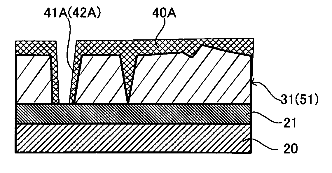
[0207]As shown in FIG. 6A, an antireflection film 21 formed of a metal thin film was formed on a semiconductor substrate 20, and an ArF resist 22 (“ARF1244J” made by JSR) was applied over the antireflection film 21, or a work surface. As shown in FIG. 6B, a halftone phase shift mask (reticle) 30 with a seal ring pattern 30A (design pattern) was then irradiated with light (ArF excimer laser light) 23, and the light passing through the reticle 30 was collected by a projection lens 24, exposing the ArF resist 22 followed by development. In this way a seal ring resist pattern—a ¼ scale image of the sealing pattern 30A in the reticle 30—was printed on the ArF resist 22. The resultant resist pattern 31 is shown in FIG. 6C. As shown in FIG. 6C, side lobes S were formed in areas other than the primary feature 31A.

—Preparation of Resist Pattern Thickening Material—

[...


PUM


Abstract

To provide a method for manufacturing a semiconductor device, which the method is capable of efficient mass production of high-performance semiconductor devices by, upon manufacture of a semiconductor device, eliminating unwanted features (e.g., side lobes) created together with a resist pattern by thickening the resist pattern, to reduce the burden in designing photomasks and to increase depth of focus. The method of the present invention for manufacturing a semiconductor device includes at least: forming a resist pattern on a work surface and applying over a surface of the resist pattern a resist pattern thickening material to thereby thicken the resist pattern to eliminate an unwanted feature created together with the resist pattern.

Description

CROSS-REFERENCE TO RELATED APPLICATIONS[0001]This application is based upon and claims the benefits of the priority from the prior Japanese Patent Application No. 2006-088670 filed on Mar. 28, 2006, the entire contents of which are incorporated herein by reference.BACKGROUND OF THE INVENTION[0002]1. Field of the Invention[0003]The present invention relates to a method for manufacturing a semiconductor device, which the method is capable of efficient mass production of high-performance semiconductor devices by, upon manufacture of a semiconductor device, eliminating unwanted features (e.g., side lobes) created together with a resist pattern by thickening the resist pattern, to reduce the burden in designing photomasks and to increase depth of focus.[0004]2. Description of the Related Art[0005]As the packing density of integrated circuits has increased in recent years, so too has the requirement for semiconductor device manufacturing equipment to achieve smaller feature size—patterns ...

Claims


Application Information

Patent Timeline
Patent Type & Authority Patents(United States)
IPC IPC(8): H01L21/461
CPCG03F7/40H01L21/0271H01L21/0276
Inventor SETTA, YUJIYAMAMOTO, HAJIME
Owner FUJITSU SEMICON LTD
Why Eureka
Try Eureka