GMR magnetic sensing element having an antiferromagnetic layer extending beyond the track width and method for making the same

a magnetic sensing element and antiferromagnetic layer technology, applied in the field of magnetic sensing elements, can solve the problems of reducing the quality of the magnetic sensing element, difficult to remove the resist layer rb>1/b>, and reducing the magnetic detection outpu

Inactive Publication Date: 2006-05-23
TDK CORPARATION
View PDF15 Cites 104 Cited by
  • Summary
  • Abstract
  • Description
  • Claims
  • Application Information

AI Technical Summary

Benefits of technology

[0076]Preferably, in step (a), the protective layer is formed using at least one element selected from the group consisting of Ru, Rh, Ir, Cr, Re and Cu. In this manner, the thickness of the oxide layer at the surface of the protective small is small, i.e., 3 to 6 Å, facilitating removal of the oxide layer.

Problems solved by technology

Furthermore, the redeposition layers A degrade the quality of the magnetic sensing element.
Moreover, the resist layer R1 is difficult to remove.
These will result in a decrease in the magnetic detection outputs and poor in asymmetry of the output since the longitudinal bias magnetic fields cannot be stably supplied to the free magnetic layer 5.

Method used


Image

  • GMR magnetic sensing element having an antiferromagnetic layer extending beyond the track width and method for making the same
  • GMR magnetic sensing element having an antiferromagnetic layer extending beyond the track width and method for making the same
  • GMR magnetic sensing element having an antiferromagnetic layer extending beyond the track width and method for making the same

Examples


first embodiment

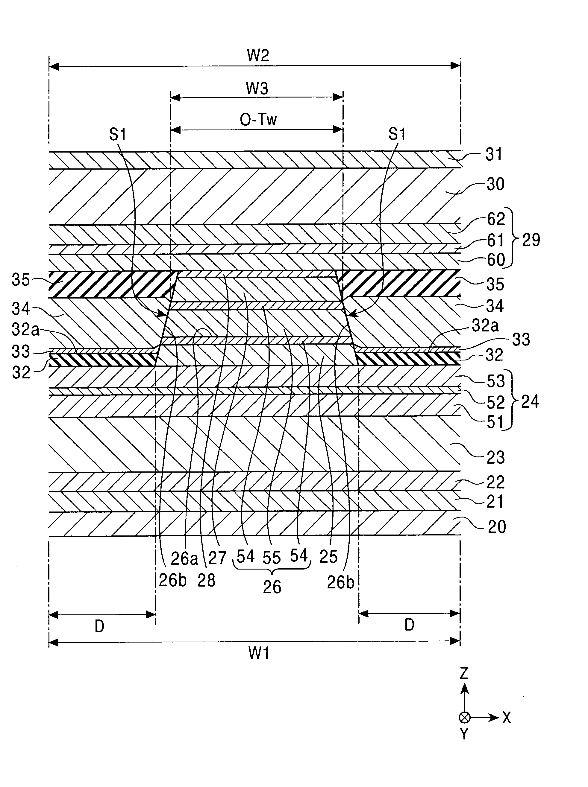
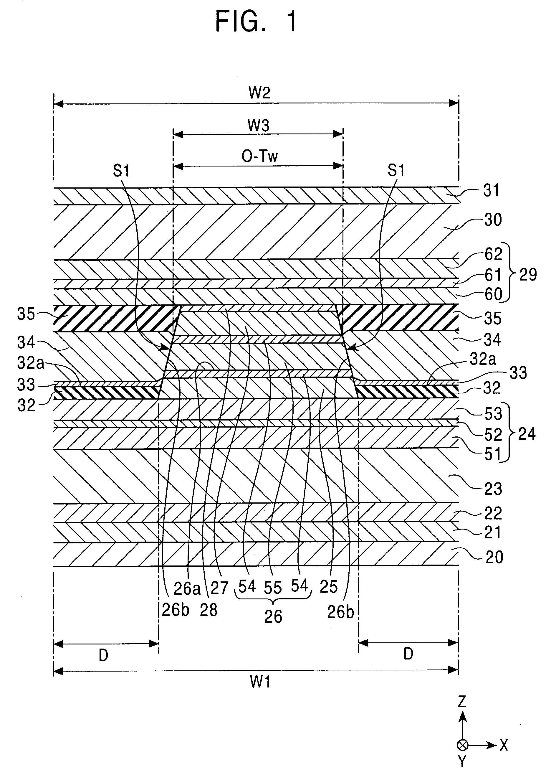
[0104]FIG. 1 is a cross-sectional view showing an overall structure of a magnetic sensing element according to a first embodiment of the present invention viewed from the opposing face. The magnetic sensing element is of a dual spin-valve type.

[0105]The magnetic sensing element includes a first electrode layer 20 composed of, for example, α-Ta, Au, Cr, Cu, or W.

[0106]An underlayer 21 is formed on the upper face of the first electrode layer 20. The underlayer 21 is preferably composed of at least one of Ta, Hf, Nb, Zr, Ti, Mo and W. The thickness of the underlayer 21 is 50 Å or less. Alternatively, no underlayer 21 may be formed.

[0107]A seed layer 22 is disposed on the underlayer 21. The seed layer 22 is mainly face-centered cubic and has the (111) faces preferentially oriented in a direction parallel to the interface with a lower antiferromagnetic layer 23 described below. The seed layer 22 is preferably composed of elemental Cr, a NiFe alloy, or a Ni—Fe—Y alloy wherein Y is at leas...

second embodiment

[0187]FIG. 4 is a cross sectional view showing the overall structure of a dual spin-valve magnetic sensing element according to a second embodiment of the present invention viewed from the opposing face.

[0188]The magnetic sensing element shown in FIG. 4 differs from the magnetic sensing element shown in FIG. 1 in that the current limiting layer 28 is formed within an upper nonmagnetic material layer 70.

[0189]The upper nonmagnetic material layer 70 is constituted from a lower sublayer 71 and an upper sublayer (second nonmagnetic material layer) 72. The two side faces of the lower sublayer 71 are flush with the two side faces of the free magnetic layer 26 and the two side faces of the current limiting layer 28. The two side faces of the upper sublayer 72 are flush with the two side faces of the upper pinned magnetic layer 29 and the two side faces of the upper antiferromagnetic layer 30. The lower sublayer 71 and the upper sublayer 72 are both composed of copper.

[0190]The current limi...

third embodiment

[0193]FIG. 5 is a cross-sectional view showing the overall structure of a magnetic sensing element according to a third embodiment of the present invention viewed from the opposing face.

[0194]The magnetic sensing element shown in FIG. 5 includes a Ta underlayer 80 formed on the first electrode layer 20, a free magnetic layer 81, a nonmagnetic material layer 82, a current limiting layer 83, a pinned magnetic layer 84, an antiferromagnetic layer 85, and the second electrode layer 31, sequentially stacked on the underlayer 80.

[0195]The first electrode layer 20 and the second electrode layer 31 are composed of the same material and have the same thickness as those of the first electrode layer 20 and the second electrode layer 31 shown in FIG. 1.

[0196]The underlayer 80 controls the crystal orientation of the free magnetic layer 81 to improve the magnetic characteristics and to reduce the resistivity of the free magnetic layer 81.

[0197]In FIG. 5, the free magnetic layer 81 is a single mag...


PUM

PropertyMeasurementUnit
lengthaaaaaaaaaa
areaaaaaaaaaaa
temperatureaaaaaaaaaa

Abstract

A magnetic sensing element with improved magnetic detection output and a method for making the same are provided. In the magnetic sensing element, the length of an upper pinned magnetic layer an upper antiferromagnetic layer in a track width direction is larger than the length of a free magnetic layer in the track width direction. In making the magnetic sensing element, there is no need to remove side portions of the upper pinned magnetic layer and the upper antiferromagnetic layer. The materials of the upper pinned magnetic layer and the upper antiferromagnetic layer are thus prevented from redepositing on two side faces of the free magnetic layer during milling.

Description

BACKGROUND OF THE INVENTION[0001]1. Field of the Invention[0002]The present invention generally relates to magnetic sensing elements for use in magnetic sensors and hard disks and methods for making the same. In particular, it relates to a magnetic sensing element that can be readily used with narrower tracks and that has improved sensitivity to magnetic fields, and to a method for making the same.[0003]2. Description of the Related Art[0004]FIG. 24 is a cross-sectional view of a conventional spin-valve magnetic sensing element viewed from a face that opposes a recording medium. Hereinafter, this face is referred to as the “opposing face”.[0005]The magnetic sensing element includes a composite film 9 constituted from an antiferromagnetic layer 2, a pinned magnetic layer 3, a nonmagnetic material layer 4, a free magnetic layer 5, a nonmagnetic material layer 6, a pinned magnetic layer 7, and an antiferromagnetic layer 8; an electrode layer 1 at the bottom of the composite film 9; an ...

Claims


Application Information

Patent Timeline
Patent Type & Authority Patents(United States)
IPC IPC(8): G11B5/39G01R33/09G11B5/31H01F10/32H01F41/18H01L43/08H01L43/10H01L43/12
CPCB82Y10/00B82Y25/00G11B5/3903G01R33/093Y10T29/49044G11B5/3116
Inventor NISHIYAMA, YOSHIHIRO
Owner TDK CORPARATION
Why Eureka
Try Eureka