Resist pattern thickening material, method for forming resist pattern, semiconductor device and method for manufacturing the same

a technology of resist pattern and thickening material, which is applied in the direction of photosensitive materials, instruments, photomechanical equipment, etc., can solve the problems of difficult control of reaction amount, difficult to use such aqueous solution material, and difficult to set up a new process line for a new chemical agent, etc., and achieves thickening resist pattern, less dependency, and excellent resist pattern particularly in etch resistance

Active Publication Date: 2013-04-16
FUJITSU LTD
View PDF52 Cites 2 Cited by
  • Summary
  • Abstract
  • Description
  • Claims
  • Application Information

AI Technical Summary

Benefits of technology

[0024]After the resist pattern thickening material is applied over the surface of a resist pattern, the resist pattern thickening material residing near the interface with the resist pattern infiltrates into the resist pattern to interact with or be mixed with the material of the resist pattern, and the compound represented by the General Formula (1) reacts to the resin residing near the compound. At this point in time, a surface layer or a mixing layer which is formed as a result of an interaction between the resist pattern thickening material and the resist pattern can be efficiently formed on the surface of the resist pattern in a state where the resist pattern constitutes the innerlayer thereof because of excellent affinity between the resist pattern thickening material and the resist pattern. As the result, the resist pattern can be efficiently thickened with the resist pattern thickening material. The thus thickened (hereinafter, may be referred to as “swelled”) resist pattern (hereinafter, may be referred to as “thickened resist pattern”) is uniformly thickened with the resist pattern thickening material. For this reason, a space pattern of resist (hereinafter, may be sometimes referred to as “space pattern”) to be formed with the thickened resist pattern has a fine structure, exceeding the exposure limit (resolution limit) of light source of an available exposure device. Since the resist pattern thickening material of the present invention contains a compound represented by the General Formula (1), the resist pattern thickening material can exhibit an effect of thickening a resist pattern efficiently and uniformly, irrespective of the type and the size of a material used for the resist pattern and has less dependency on the type and the size of the material used for the resist pattern. When a phenol resin, polyvinylpyrolidone, and the like are used as the resin, the resist pattern is excellent particularly in etch resistance because the resin and the compound represented by the General Formula (1) respectively have an aromatic ring. For this reason, the resist pattern thickening material of the present invention can also be preferably used in forming a resist pattern such as a lines & spaces pattern on an interconnection layer of a LOGIC LSI in which various sizes of thickened resist patterns are utilized.
[0028]In the method for manufacturing a semiconductor device of the present invention, in the forming of a resist pattern, a resist pattern is formed on a surface of a workpiece to which a pattern such as an interconnection pattern is to be formed, and the above-noted resist pattern thickening material is applied so as to cover the surface of the resist pattern. Then, the resist pattern thickening material residing near the interface with the resist pattern infiltrates into the resist pattern to interact with or be mixed with the material of the resist pattern, and the compound represented by the General Formula (1) reacts to the resin residing near the compound. Then, a surface layer or a mixing layer formed as a result of an interaction between the resist pattern thickening material and the resist pattern can be efficiently formed on the surface of the resist pattern in a state where the resist pattern constitutes the innerlayer thereof. The thus thickened resist pattern is uniformly thickened with the resist pattern thickening material. For this reason, a space pattern of resist formed with the thickened resist pattern has a fine structure, exceeding the exposure limit (resolution limit) of light sources of an available exposure device. Since the resist pattern thickening material of the present invention contains a compound represented by the General Formula (1), the resist pattern thickening material can exhibit an effect of thickening the resist pattern efficiently and uniformly, irrespective of the type and the size of a material used for the resist pattern and has less dependency on the type and the size of the material used for the resist pattern. When a phenol resin, polyvinylpyrolidone and the like are used as the resin, the resist pattern is excellent particularly in etch resistance because the resin and the compound represented by the General Formula (1) respectively have an aromatic ring. Therefore, with the use of the resist pattern thickening material of the present invention, it is possible to easily and precisely form a thickened resist pattern such as a lines & spaces pattern on an interconnection layer of a LOGIC LSI where not only a contact hole pattern but also various sizes of thickened resist patterns are utilized.
[0029]Subsequently, in the patterning of the thickened resist pattern, by etching the surface of the workpiece using the thickened resist pattern which has been thickened in the forming of the resist pattern, the surface of the workpiece can be patterned finely and precisely with accurate dimension, thus high quality and high performance semiconductor devices each having a pattern such as an extremely fine and precise interconnection pattern with excellent accurate dimension can be manufactured efficiently.
[0030]The semiconductor device of the present invention is manufactured by the method for manufacturing a semiconductor device of the present invention. The semiconductor device has patterns, for example, interconnection patterns, with fine, precise and accurate dimension, and is of high quality and of high performance.

Problems solved by technology

However, the type of chemical agents that can be linked to a coater / developer track to be used in semiconductor process at present is limited to resist materials and rinse solutions, and it is very difficult to set up a new process line for a new chemical agent.
In the conventional semiconductor process, it is not based on the assumption that an aqueous solution material is applied over a surface of a resist pattern, and thus it is also difficult to use such an aqueous solution material because of the necessity of a new control for waste fluid.
In addition, with the use of such a conventional material composition utilizing a crosslinking reaction, it is difficult to control the amount of reaction, and there are the following shortcomings.
It is liable to cause differences in the amount of reaction depending on the initial pattern size of a resist pattern, loss of a resist pattern caused by an embedded space pattern of resist dependence of the amount of reaction on the used pattern shape and the like, and the process margin is narrow.
In the meanwhile, when a pattern is formed utilizing an X-ray, an electron beam, or the like, each of which has a further shorter wavelength than that of the ArF (argon fluoride) excimer laser light (wavelength: 193 nm), it results in a high-cost and a low-productivity.
With the use of the composition for the aqueous solution material described in Japanese patent Application Laid Open (JP-A) No. 11-283910, it has been known that the use of the aqueous solution material composition is not effective in thickening (swelling) an ArF resist pattern containing a resin which is different from the resin used for KrF resist patterns, although it is effective in thickening (swelling) a KrF resist pattern using a phenol resin, and there is a problem that the aqueous solution material composition cannot be utilized for ArF resists which are typically used for processing advanced devices.
Furthermore, a reduced resist pattern using the polyvinyl acetal resin as a base, which is obtained by the technique described in Japanese Patent Application Laid-Open (JP-A) No. 11-283910 may be sometimes insufficient in dry etch resistance to cause a problem with processability.
In the meanwhile, in case of a resist pattern using the silicone resin as a base, an etching residue of the silicone resin occurs, and therefore it is often needed to further remove the residue, and the resist pattern is not practical, although the dry etch resistance thereof is satisfactorily provided.

Method used


Image

  • Resist pattern thickening material, method for forming resist pattern, semiconductor device and method for manufacturing the same
  • Resist pattern thickening material, method for forming resist pattern, semiconductor device and method for manufacturing the same
  • Resist pattern thickening material, method for forming resist pattern, semiconductor device and method for manufacturing the same

Examples


example 1

Preparation of Resist Pattern Thickening Material

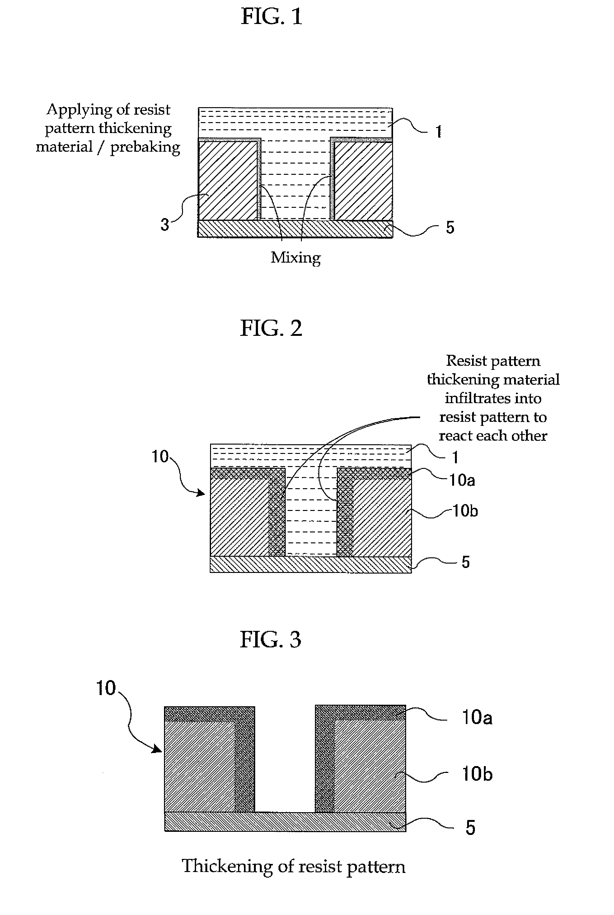
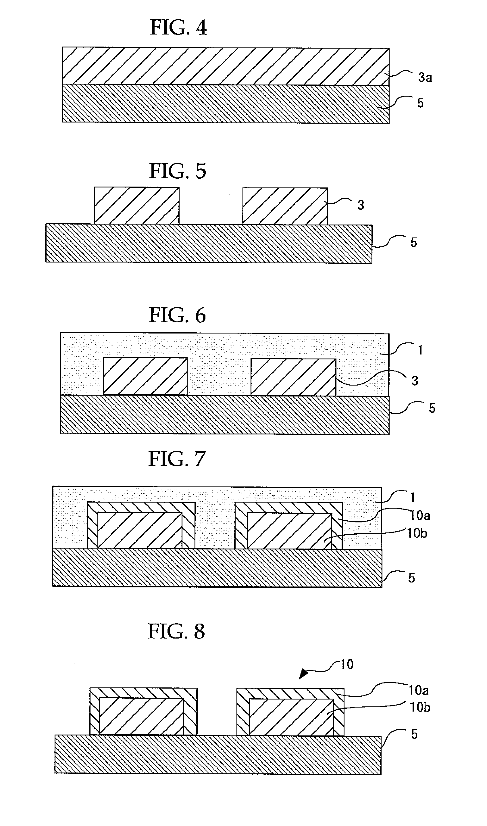
[0153]Resist pattern thickening materials A to O each having a composition shown in Table 1, each of which was a nonaqueous material and contained no acid generator and no crosslinker were prepared.

[0154]Note that “Thickened material” shown in Table 1 means a resist pattern thickening material, and the letters of “A” to “O” respectively correspond to the resist pattern thickening materials A to O. In the resist pattern thickening materials A to O, the resist pattern thickening material A corresponds to a material for Comparative Examples, and the resist pattern thickening materials B to O respectively correspond to materials for Examples of the present invention. The unit of values shown in parentheses in Table 1 is “part by mass” or “parts by mass”.

[0155]In the column “Compound represented by General Formula (1)” for the resist pattern thickening materials B to O, “benzyl alcohol”, “benzyl amine” and “the derivative thereof (a deriva...

example 2

Formation of Resist Pattern

[0163]Each of the resist pattern thickening materials A to O prepared in Example 1 was applied over a surface of a hole pattern which had been formed from an ArF resist (“AR 1244J”, manufactured by JSR CORPORATION), the hole pattern having an opening diameter described in the column “Size of unthickened space pattern of resist (before thickening)” in Table 2, by a spin-coating method under the conditions of 1,000 rpm / 5 s initially, and subsequently, 3,500 rpm / 40 s. Then, the each of the applied resist pattern thickening material was baked under the condition of 110° C. / 60 s. Next, each of the applied resist pattern thickening materials A to E, J, K, L and N was rinsed with 2.38% by mass of a TMAH alkali developer for 60 seconds and further rinsed with pure water for 60 seconds, and each of the applied resist pattern thickening materials F to I, M and O was rinsed with pure water or 2.38% by mass of a TMAH alkali developer for 60 seconds and further rinsed ...

example 3

Formation of Resist Pattern

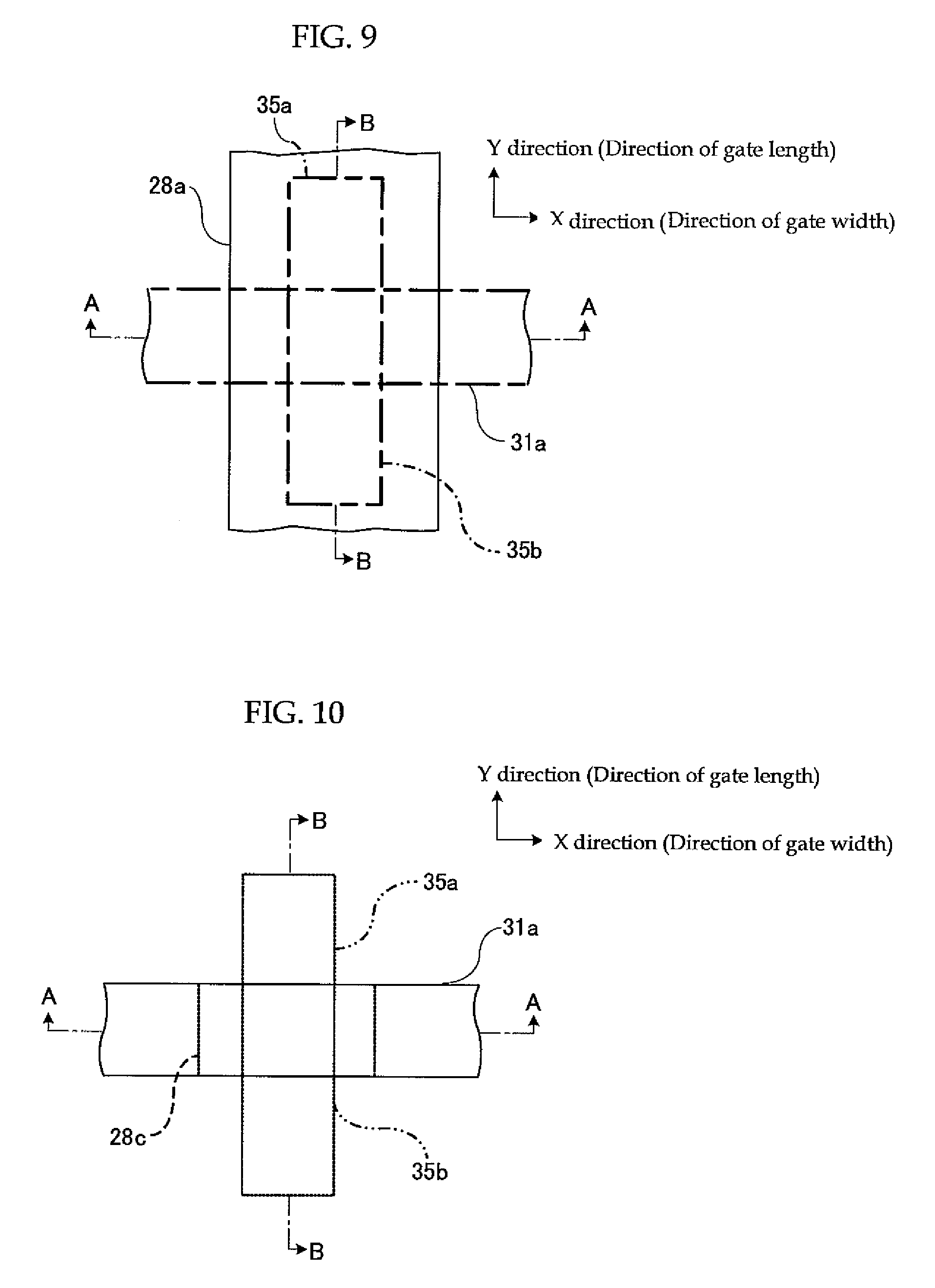
[0167]Each of the resist pattern thickening materials D and G prepared in Example 1 was applied over a surface of a lines & spaces pattern which had been formed from an ArE resist (“AR 1244J”, manufactured by JSR CORPORATION), the lines & spaces patterns respectively had a space portion having a varied size (the size described in the column “Size of unthickened space pattern of resist (before thickening)” in Table 2, i.e., 110 nm, 200 nm, 300 nm, and 500 nm), by a spin-coating method under the conditions of 1,000 rpm / 5 s initially, and subsequently, 3,500 rpm / 40 s. Then, the each of the applied resist pattern thickening material was baked under the condition of 110° C. / 60 s. Next the applied resist pattern thickening material D was rinsed with 2.38% by mass of a TMAH alkali developer for 60 seconds and further rinsed with pure water for 60 seconds. The applied resist pattern thickening material G was rinsed with pure water for 60 seconds and further rinsed...


PUM

PropertyMeasurementUnit
wavelengthaaaaaaaaaa
boiling pointaaaaaaaaaa

Abstract

The present invention provides a resist pattern thickening material, which can utilize ArF excimer laser light; which, when applied over a resist pattern to be thickened, e.g., in form of lines and spaces pattern, can thicken the resist pattern to be thickened regardless of the size of the resist pattern to be thickened; and which is suited for forming a fine space pattern or the like, exceeding exposure limits. The present invention also provides a process for forming a resist pattern and a process for manufacturing a semiconductor device, wherein the resist pattern thickening material of the present invention is suitably utilized.

Description

CROSS-REFERENCE TO RELATED APPLICATIONS[0001]This application is based upon and claims the benefits of the priority from the prior Japanese Patent Application Nos. 2006-260854 filed on Sep. 26, 2006 and 2007-189182 filed on Jul. 20, 2007 the entire contents of which are incorporated herein by reference.BACKGROUND OF THE INVENTION[0002]1. Field of the Invention[0003]The present invention relates to a resist pattern thickening material capable of forming a fine space pattern of resist, exceeding exposure limits (resolution limits) of light sources of available exposure devices by thickening a resist pattern to be formed when manufacturing a semiconductor device, and the present invention also relates to a method for forming a resist pattern, a semiconductor device, and a method for manufacturing the semiconductor device.[0004]2. Description of the Related Art[0005]Semiconductor integrated circuits are becoming more highly integrated, and LSIs and VLSIs are increasingly being put into ...

Claims


Application Information

Patent Timeline
Patent Type & Authority Patents(United States)
IPC IPC(8): G03F7/004
CPCC08K5/17G03F7/40H01L21/0273H01L21/31144H01L29/06H01L27/11526H01L27/11543G03F7/38H01L21/3081H01L27/105H01L21/0338H10B41/40H10B41/48G03F7/0045G03F7/0047H01L21/027
Inventor NOZAKI, KOJIKOZAWA, MIWA
Owner FUJITSU LTD
Why Eureka
Try Eureka