

Semiconductor device and method of manufacturing the same
a technology of semiconductor devices and semiconductors, applied in semiconductor devices, instruments, electrical devices, etc., can solve the problems of difficult to obtain an element having sufficient performance, difficult to control the ldd region, and the most important problem of ldd region control, etc., to achieve high mass productivity, high reliability, and high reproducibility
- Summary
- Abstract
- Description
- Claims
- Application Information
AI Technical Summary
Benefits of technology
Problems solved by technology
Method used
Image

Examples
embodiment 1
[Embodiment 1]
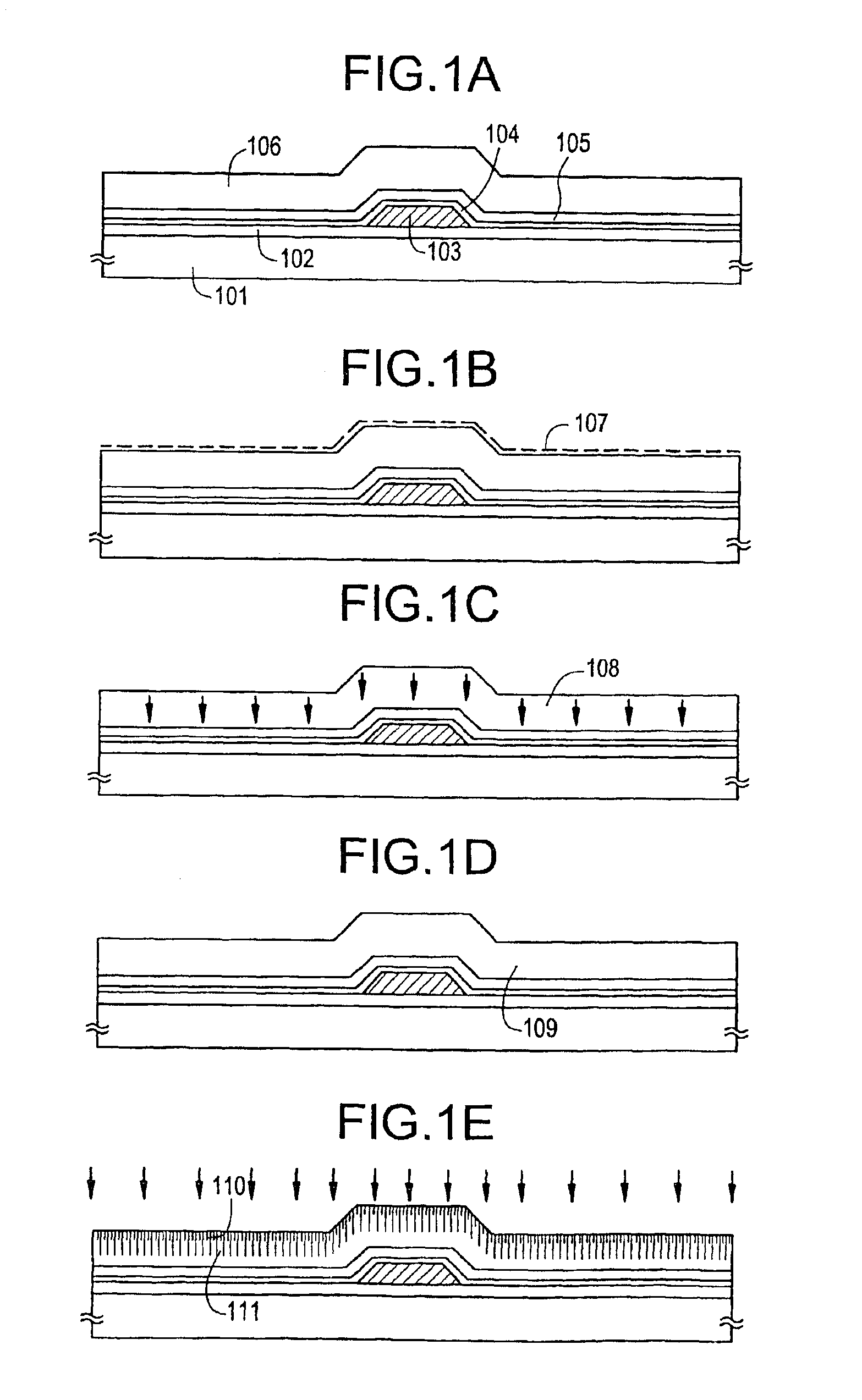
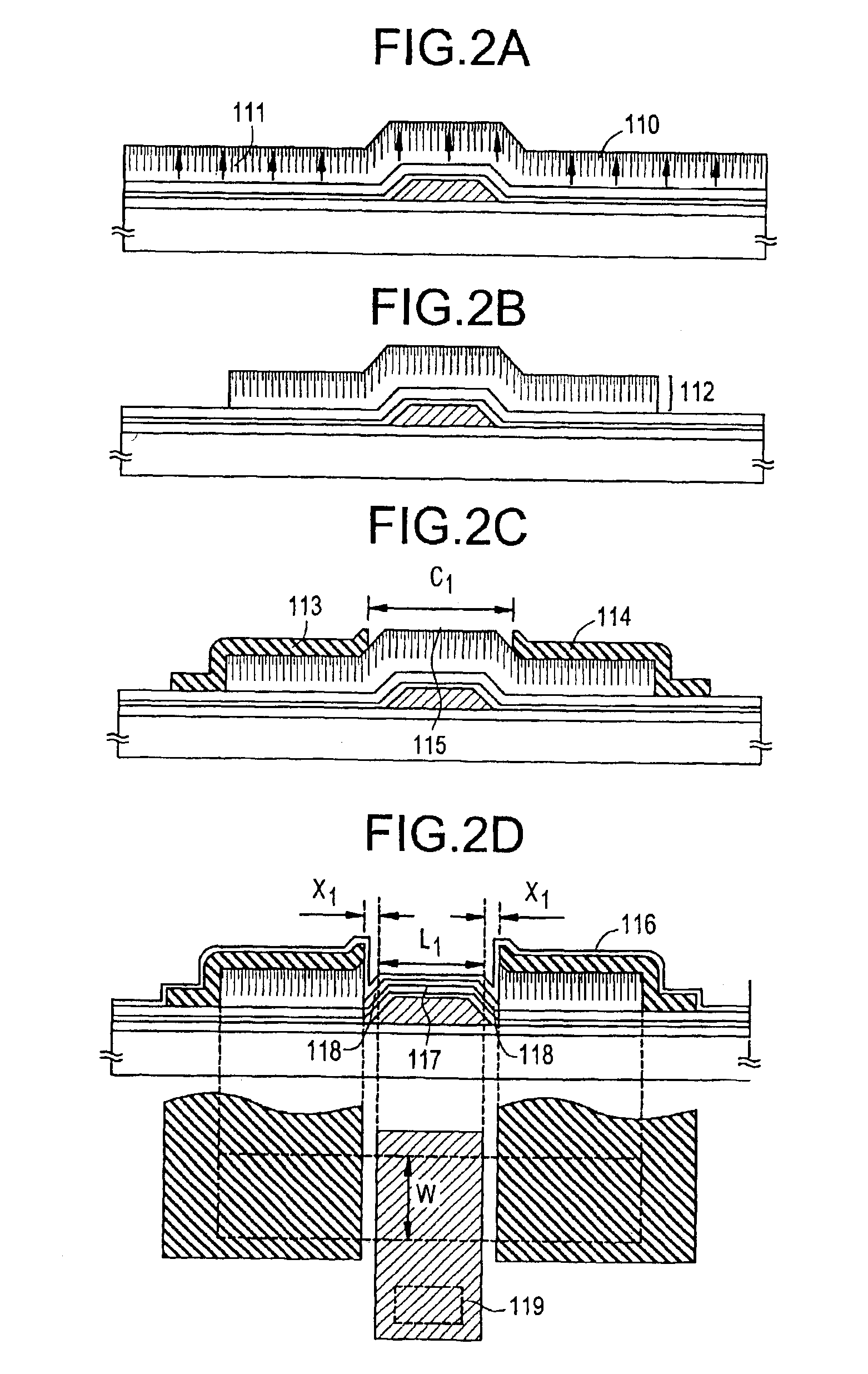
[0068]A first embodiment of the present invention will be described with reference to FIGS. 1A-1E, 2A-2D, and 3. First, a method of manufacturing a semiconductor device of the present invention will be described with reference to FIGS. 1A to 1E.
[0069]An under film made of an insulating film containing silicon as the main ingredient is formed on a glass substrate (or quartz substrate, silicon substrate) 101. A gate electrode (first wiring) 103 made of a conductive film is formed thereon.
[0070]The line width of the gate electrode 103 is made 1 to 10 μm (typically 3 to 5 μm). The film thickness thereof is made 200 to 500 nm (typically 250 to 300 nm). In this embodiment, the gate electrode with a line width of 3 μm is formed by using a lamination film (for example, Ta / TaN) of a Ta (tantalum) film with a thickness of 250 nm and a TaN (tantalum nitride) film with a thickness of 250 nm.
[0071]For the gate electrode 103, a material (tantalum, tungsten, titanium, chromium, molyb...
embodiment 2
[Embodiment 2]
[0128]In this embodiment, in the structure of the present invention, an example of a structure different from the embodiment 1 will be described. Since the manufacturing steps of the TFT may follow the embodiment 1, only necessary portions will be described in this embodiment.
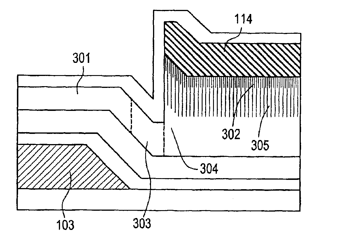
[0129]First, in accordance with the manufacturing steps of the embodiment 1, the state shown in FIG. 5A is obtained. The point different from the embodiment 1 is that when a source electrode 501 and a drain electrode 502 are formed, the length of a channel etching region 500 is made C2. At this time, the length C2 is shorter than a gate electrode width and is determined within the range of 2 to 9 μm (typically 2 to 4 μm). That is, the feature of this embodiment is to provide electrodes such that the gate electrode and the source / drain electrodes overlap with each other.
[0130]In this state, when a channel etching step is carried out as described in the embodiment 1 and a protective film is provided...
embodiment 3
[Embodiment 3]
[0137]In this embodiment, in the structure of the present invention, an example of structure different from the embodiments 1 and 2 will be described. Since manufacturing steps of a TFT may basically follow the embodiment 1, only necessary portions will be described in this embodiment.
[0138]First, in accordance with the manufacturing steps of the embodiment 1, the state shown in FIG. 6A is obtained. Here, the different point from the embodiment 1 is that the length of a channel etching region 600 is made C3 when a source electrode 601 and a drain electrode 602 are formed. At this time, since the length C3 is made to coincide with the width of a gate electrode, the length becomes 1 to 10 μm (typically 3 to 5 μm).
[0139]In this state, when a channel etching step is carried out as described in the embodiment 1 and a protective film is provided, the state shown in FIG. 6B is obtained. At this time, a region designated by 603 becomes a channel formation region, and its chann...
PUM
| Property | Measurement | Unit |
|---|---|---|
| thickness | aaaaa | aaaaa |
| thickness | aaaaa | aaaaa |
| thickness | aaaaa | aaaaa |
Abstract
Description
Claims
Application Information