Method for manufacturing semiconductor device

a semiconductor film and manufacturing method technology, applied in the field of display devices, can solve the problems of increased cost, reduced yield, and complicated process of transistor using polycrystalline semiconductor films, and achieve the effect of excellent electric characteristics and high reliability

Inactive Publication Date: 2009-01-08
SEMICON ENERGY LAB CO LTD
View PDF30 Cites 39 Cited by
  • Summary
  • Abstract
  • Description
  • Claims
  • Application Information

AI Technical Summary

Benefits of technology

[0008]In view of the above problems, it is an object of the present invention to provide a method for manufacturing a display device having a thin film transistor which has excellent electric characteristics and high reliability, with high mass productivity.
[0026]According to the present invention, a display device having a thin film transistor with excellent electric characteristics and high reliability can be manufactured.

Problems solved by technology

However, the thin film transistor using a polycrystalline semiconductor film requires a more complicated process than the thin film transistor using an amorphous semiconductor film because of crystallization of the semiconductor film.
Thus, there are problems such as a reduction in yield and an increase in cost.

Method used


Image

  • Method for manufacturing semiconductor device
  • Method for manufacturing semiconductor device
  • Method for manufacturing semiconductor device

Examples


embodiment mode 1

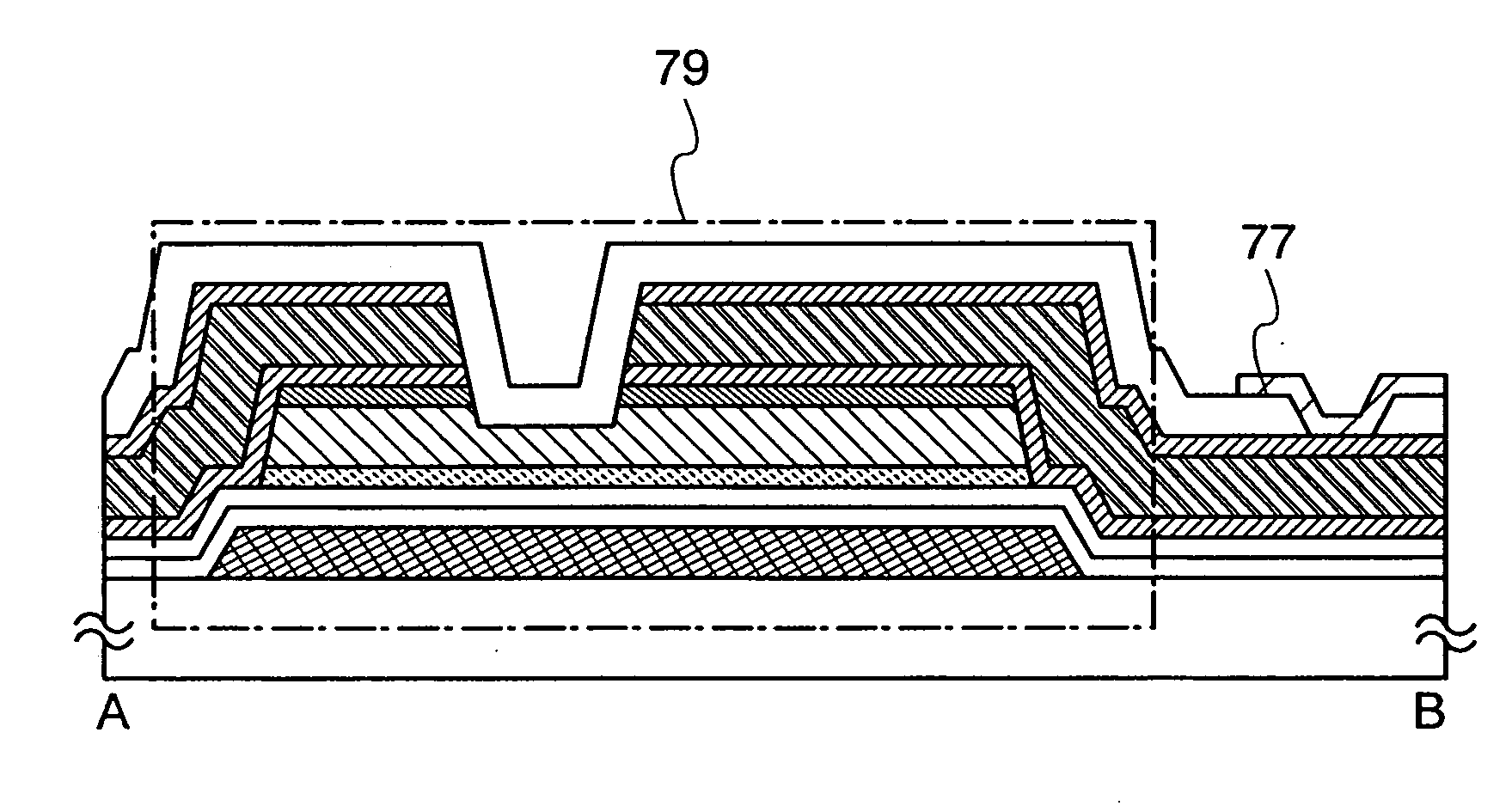
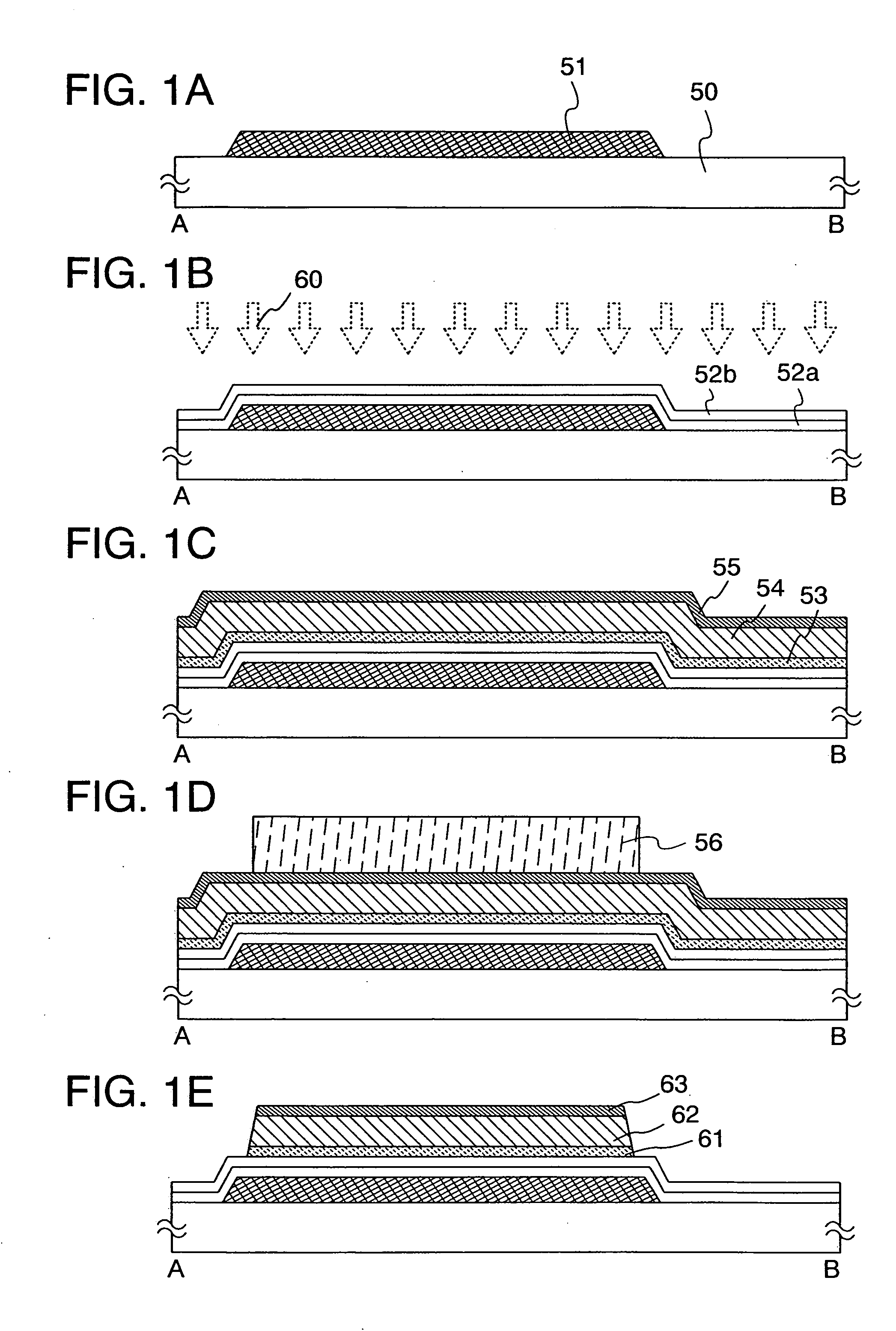
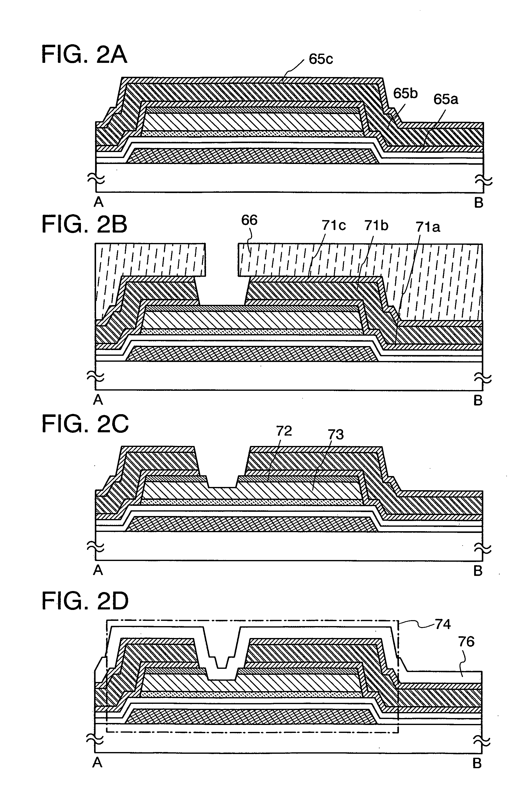
[0055]This embodiment mode describes a manufacturing process of a thin film transistor used for a display device, with reference to FIGS. 1A to 1E, FIGS. 2A to 2D, FIGS. 3A and 3B, and FIGS. 4A to 4D. FIGS. 1A to 1E, FIGS. 2A to 2D, and FIGS. 3A and 3B are cross-sectional views illustrating a manufacturing process of a thin film transistor. FIGS. 4A to 4D are plan views of a connection region of a thin film transistor and a pixel electrode in one pixel, and FIGS. 1A to 1E, FIGS. 2A to 2D, and FIGS. 3A and 3B are cross-sectional views illustrating a manufacturing process of a thin film transistor which are taken along line A-B in FIGS. 4A to 4D.

[0056]As for a thin film transistor having a microcrystalline semiconductor film, an n-type thin film transistor has higher mobility than a p-type thin film transistor; thus, an n-type thin film transistor is more suitable for a driver circuit. However, in the present invention, either an n-type or p-type thin film transistor can be used. With...

embodiment mode 2

[0111]This embodiment mode describes an example in which a step of forming a microcrystalline semiconductor film is different from that in Embodiment Mode 1. Therefore, other steps can be performed in a manner similar to Embodiment Mode 1, and the same portion or a portion having the same function, and the same steps as in Embodiment Mode 1 are not repeatedly explained.

[0112]First, the gate electrode 51 is formed over the substrate 50 in a manner similar to Embodiment Mode 1, and the gate insulating films 52a and 52b are formed.

[0113]In this embodiment mode, hydrogen plasma treatment performed on the gate insulating film 52b and a step of forming the microcrystalline semiconductor film are separately carried out. First, the hydrogen plasma treatment is performed on the surface of the gate insulating film 52b. The microcrystalline semiconductor film may be formed over the gate insulating film which is subjected to hydrogen plasma treatment, with the use of a deposition gas including ...

embodiment mode 3

[0116]This embodiment mode describes an example in which a step of manufacturing a display device is different from Embodiment Mode 1 or 2. Therefore, other steps can be performed in a manner similar to Embodiment Mode 1 or 2. The same portion or a portion having the same function and the same steps as in Embodiment Mode 1 are not repeatedly explained.

[0117]In Embodiment Mode 1, before the microcrystalline semiconductor film is formed, a reaction chamber may be subjected to cleaning and flush (washing) treatment (hydrogen flush using hydrogen as a flush substance, silane flush using silane as a flush substance, or the like). By the flush treatment, a film to be formed can be prevented from being contaminated by an impurity such as oxygen, nitrogen, or fluorine in a reaction chamber.

[0118]By the flush treatment, an impurity such as oxygen, nitrogen, or fluorine in a reaction chamber can be removed. For example, flush treatment is performed in the following manner: a plasma CVD appara...


PUM

PropertyMeasurementUnit
thicknessaaaaaaaaaa
thicknessaaaaaaaaaa
energy gap Egaaaaaaaaaa

Abstract

A method for manufacturing a semiconductor device is provided, which comprises at least a steps of forming a gate insulating film over a substrate, a step of forming a microcrystalline semiconductor film over the gate insulating film, and a step of forming an amorphous semiconductor film over the microcrystalline semiconductor film. The microcrystalline semiconductor film is formed by introducing a silicon hydride gas or a silicon halide gas when a surface of the gate insulating film is subjected to hydrogen plasma to generate a crystalline nucleus over the surface of the gate insulating film, and by increasing a flow rate of the silicon hydride gas or the silicon halide gas.

Description

BACKGROUND OF THE INVENTION[0001]1. Field of the Invention[0002]The present invention relates to a display device using a thin film transistor at least for a pixel portion.[0003]2. Description of the Related Art[0004]In recent years, a technique that is used to form thin film transistors using semiconductor thin films (with thicknesses of from several nanometers to several hundreds of nanometers, approximately) formed over substrates having an insulating surface has been attracting attention. Thin film transistors are applied to a wide range of electronic devices such as ICs or electro-optical devices, and prompt development of thin film transistors that are to be used as switching elements in image display devices, in particular, is being pushed.[0005]As a switching element in an image display device, a thin film transistor using an amorphous semiconductor film, a thin film transistor using a polycrystalline semiconductor film, or the like is used. As a method for forming a polycry...

Claims


Application Information

Patent Timeline
Patent Type & Authority Applications(United States)
IPC IPC(8): H01L21/20H01L21/336
CPCH01L29/04H01L29/41733H01L29/458H01L27/1292H01L29/66765H01L29/78678H01L29/78696H01L29/4908
Inventor YAMAZAKI, SHUNPEI
Owner SEMICON ENERGY LAB CO LTD
Why Eureka
Try Eureka