Power devices having trench-based source and gate electrodes

a technology of gate electrodes and power devices, which is applied in the direction of semiconductor devices, diodes, electrical devices, etc., can solve the problems of reducing the on-resistance of devices, and achieve the effect of improving the breakdown voltage and on-resistance of devices

Active Publication Date: 2006-03-23
INFINEON TECH AMERICAS CORP
View PDF16 Cites 153 Cited by
  • Summary
  • Abstract
  • Description
  • Claims
  • Application Information

AI Technical Summary

Benefits of technology

[0017] According to a first embodiment of the invention, an example power semiconductor device includes a semiconductor body with a highly doped drain region, a drift region of lower concentration of impurities than the drain region, and a highly doped source region, each of a first conductivity type, and a channel region of a second conductivity type disposed between the source and drift regions. The drift region may by uniformly doped or doped in a monotonically increasing fashion from the channel region towards the drift region, the variable doping improving the breakdown voltage and on-resistance of the device.

Problems solved by technology

Notably, the cellular design increases the charge coupling between the source and drift regions, thereby reducing the on-resistance of the device.

Method used


Image

  • Power devices having trench-based source and gate electrodes
  • Power devices having trench-based source and gate electrodes
  • Power devices having trench-based source and gate electrodes

Examples


Embodiment Construction

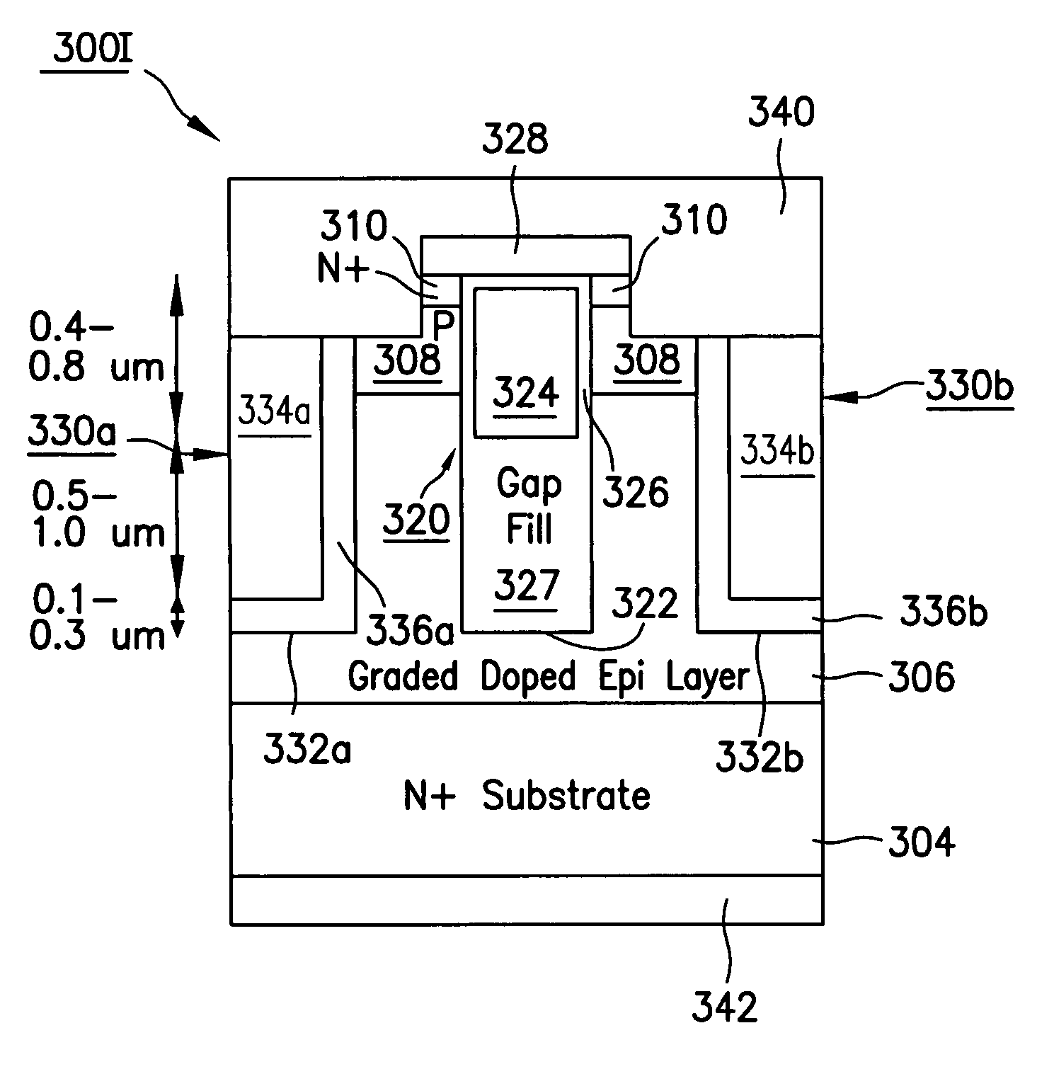
[0082] Referring to FIG. 2A, there is shown in cross section a portion of an example power semiconductor device 200A according to an embodiment of the present invention (Note that FIG. 2A and the other Figures described below are not drawn to scale). Device 200A includes a semiconductor body 202 that has a highly doped drain region 204 of a first conductivity type (e.g., N-type) and a drift region 206 of the same conductivity type, but of lower concentration of impurities, formed thereon. Formed over drift region 206 is channel region 208. Channel region 208 is of a second conductivity type opposite to that of the first conductivity type (e.g. P-type). Formed along the surface of semiconductor body 202 and over channel region 208 is a highly doped source region 210 of the first conductivity type (e.g. N-type).

[0083] According to an embodiment of the invention, drift region 206 is uniformly doped throughout. According to another embodiment of the invention, the doping in drift regio...


PUM


Abstract

A power semiconductor device includes a plurality of trenches formed within a semiconductor body, each trench including one or more electrodes formed therein. In particular, according to embodiments of the invention, the plurality of trenches of a semiconductor device may include one or more gate electrodes, may include one or more gate electrodes or one or more source electrodes, or may include a combination of both gate and source electrodes formed therein. The trenches and electrodes may have varying depths within the semiconductor body.

Description

RELATED APPLICATIONS [0001] This application is based on and claims priority to U.S. Provisional Application No. 60 / 605,340, filed on Aug. 27, 2004, by Dev Alok Girdhar, entitled, “LOW VOLTAGE MOSFET,” the contents of which are herein incorporated by reference.BACKGROUND OF THE INVENTION [0002] 1. Field of the Invention [0003] The present invention relates generally to semiconductor devices, and more specifically, to trench type power semiconductor devices. [0004] 2. Description of Related Art [0005] Trench type power semiconductor devices such as power MOSFETs are well known. As is also known, one objective in designing these devices is to obtain a low on-resistance while also obtaining a high maximum blocking voltage, also referred to as breakdown voltage. For example, referring to FIG. 1A, which is a reproduction of FIG. 5 from U.S. Pat. No. 6,649,975, by B. J. Baliga, there is shown a prior art power MOSFET 100A. (Note that S. Sapp describes a similar device in U.S. Pat. No. 6,7...

Claims


Application Information

Patent Timeline
Patent Type & Authority Applications(United States)
IPC IPC(8): H01L29/94
CPCH01L29/0878H01L29/1095H01L29/407H01L29/41766H01L29/861H01L29/42368H01L29/7805H01L29/7806H01L29/7813H01L29/4236
Inventor GIRDHAR, DEV ALOKMA, LING
Owner INFINEON TECH AMERICAS CORP
Why Eureka
Try Eureka