Method for producing epitaxial silicon wafer
a technology of epitaxial silicon and silicon wafer, which is applied in the direction of decorative surface effects, electrical appliances, decorative arts, etc., can solve the problems of reducing the yield rate of epitaxial film, and reducing the density of lpds in the front surface of epitaxial film deposited thereafter, etc., to achieve excellent gate oxide integrity, reduce friction coefficient, and reduce the density of lpds in the front surface of epitaxial film
- Summary
- Abstract
- Description
- Claims
- Application Information
AI Technical Summary
Benefits of technology
Problems solved by technology
Method used
Image
Examples
first embodiment
[0074]An embodiment of the present invention is specifically explained below. A method is explained of producing an epitaxial silicon wafer to fabricate a bipolar IC device.
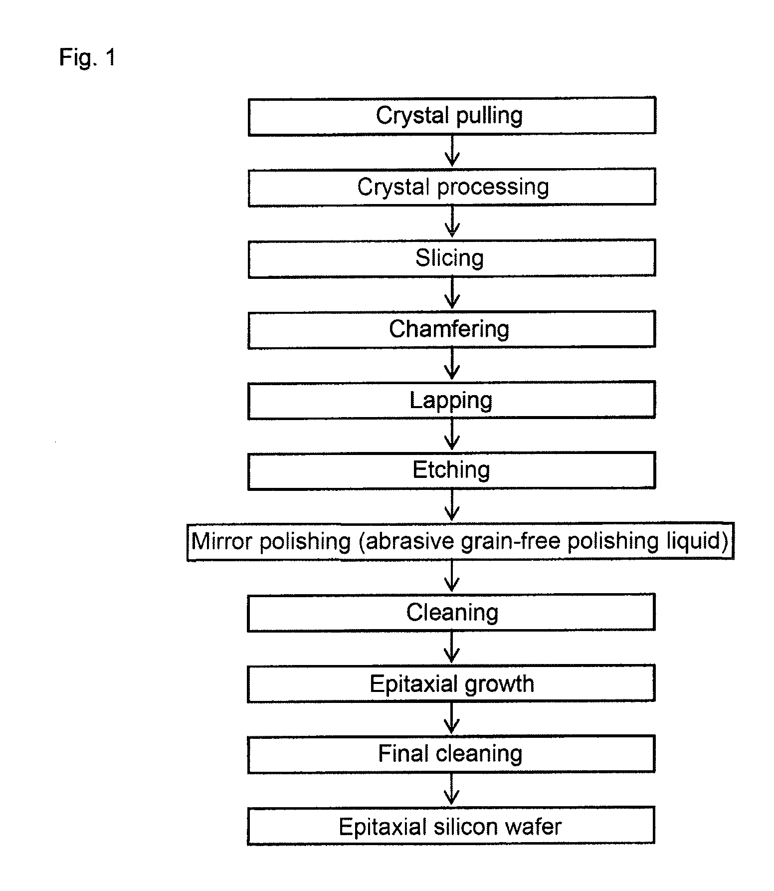
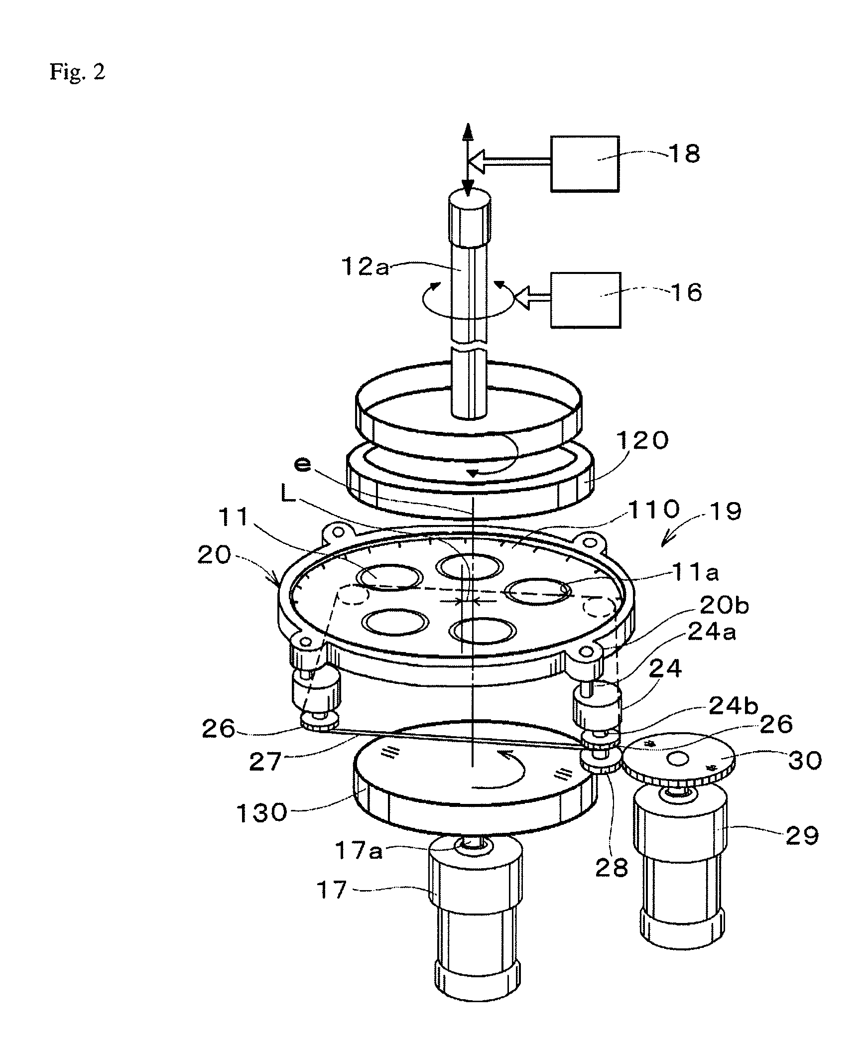
[0075]With reference to FIGS. 1 to 4, a method of producing an epitaxial silicon wafer according to the first embodiment is explained.
[0076]With reference to the flow sheet in FIG. 1, the method of producing the epitaxial silicon wafer according to the first embodiment includes crystal pulling, crystal processing, slicing, chamfering, lapping, etching, mirror-polishing, cleaning, epitaxial growth, and final cleaning.
[0077]Each process is described specifically below.
[0078]In the crystal pulling, a monocrystalline silicon ingot is pulled in the CZ process from silicon molten liquid doped with a predetermined amount of boron in a crucible, the monocrystalline silicon ingot having a diameter of 306 mm, a length of a straight body portion of 2,500 mm, a resistivity of 0.01 Ω·cm, and an initial oxygen concentration of...
second embodiment
[0103]A method of producing an epitaxial silicon wafer according to the second embodiment of the present invention is explained below with reference to FIGS. 5 to 13.
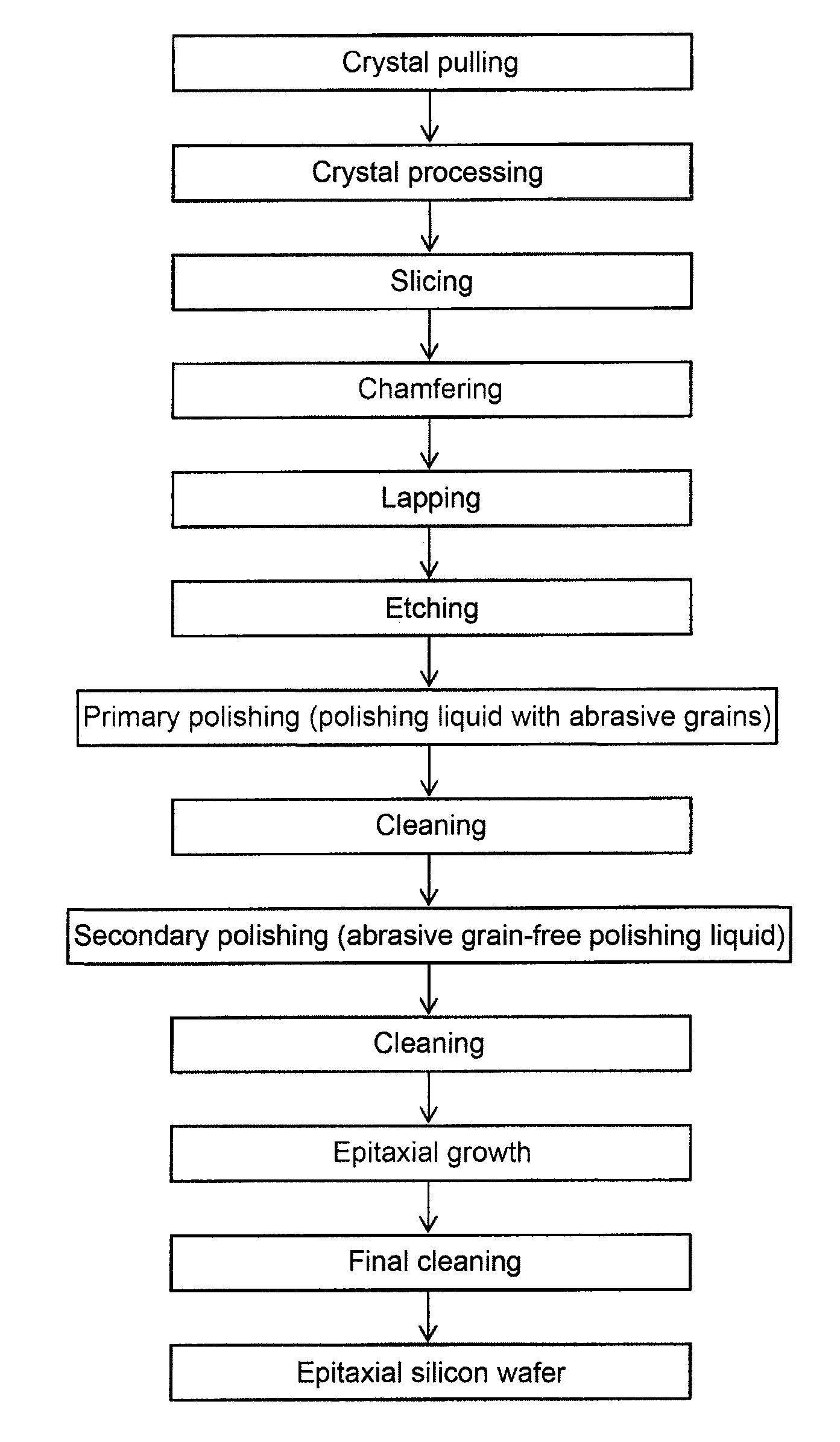
[0104]With reference to FIG. 5, the method of producing the epitaxial silicon wafer according to the second embodiment includes crystal pulling, crystal processing, slicing, chamfering, lapping, etching, primary polishing, cleaning, secondary polishing (mirror-polishing), cleaning, epitaxial growth, and final cleaning.
[0105]A no-sun gear double-side polisher used for mirror-polishing in the first embodiment is used in the primary polishing. The two polishing platens 120 and 130 are rotated in opposite directions; and the rotation speed of the polishing platens 120 and 130, the polishing pressure, and the polishing time are adjusted such that two surfaces of the silicon wafer 11 housed in the wafer housing 11a provided in the carrier plate 110 undergo simultaneous primary polishing for a polishing amount of 0.5 μm on one...
PUM
| Property | Measurement | Unit |
|---|---|---|
| pH | aaaaa | aaaaa |
| surface roughness | aaaaa | aaaaa |
| surface roughness | aaaaa | aaaaa |
Abstract
Description
Claims
Application Information


