Customized polishing pads for CMP and methods of fabrication and use thereof

a technology of polishing pads and cmp, which is applied in the direction of manufacturing tools, lapping machines, abrasive surface conditioning devices, etc., can solve the problems of increased design complexity, inability to achieve customized tribological, chemical and frictional characteristics, and the art of cmp pads, which are both open-pore and closed-pore polymeric pads, etc., to achieve the effect of reducing the number of defects, reducing the number of planarizations, and increasing the length

Active Publication Date: 2006-12-07
CMC MATERIALS INC
View PDF15 Cites 106 Cited by
  • Summary
  • Abstract
  • Description
  • Claims
  • Application Information

AI Technical Summary

Benefits of technology

[0018] The choice of pad micro-structure can have a impact on the polishing properties. Several polymers have been used in the past as polishing pad materials, which include polyolefins, polyurethanes and polycarbonates. Amongst all polymers, urethanes are used most commonly to make CMP pads. In the present invention, the pad micro-structure has been controlled through selection of appropriate polymeric components. An isocyanate prepolymer is first synthesized or commercially obtained. The isocyanate prepolymer is then reacted in with a mixture of polyamine and polyol chain extenders and polyamine and polyol curatives to complete the polymer formation. As a result, a uniform spatial distribution of alternating hard and soft domains with a long range order is obtained at the nano-micron length scale. Such a pad micro-structure can allow for a flat and extended Stribeck curve. Further, such pad structure can allow for superior control of tribological, thermal and optical properties. Accordingly, these properties can also be spatially distributed to achieve customized polishing functionality.
[0023] Surface-engineering of pads is achieved through the addition of solid lubricants and / or polymeric lubricants within the pad. Such methods of surface-engineering through lubricant addition can be used effectively to reduce the coefficient of friction while maintaining the desired removal rate. These pads can be used for most polishing applications, since a lower COF can be desirable for most applications. In particular, these surface engineered pads can be used for all the processing steps in copper CMP, which include the bulk, the soft landing and the barrier removal steps, eliminating the need for three different pads for each of the processing steps. 5) Low-Shear Integral Pads
[0025] Embedded abrasive pads may be made by incorporating abrasives within a pad during pad manufacture by techniques such as liquid casting / molding, injection molding, sintering and others. The embedded abrasive pads can have the advantage of eliminating the need for the addition of abrasives to the slurry, by providing these abrasives through the pad composition. Embedded abrasive pads can comprise individual abrasive particles and also block copolymers, where the block copolymer has a differing constituent abrasive polymeric composition in the block copolymer over distance. 7) In Situ Grooved Pads

Problems solved by technology

The current art of CMP pads, which are both open-pore and closed-pore polymeric pads, are not tailored to achieve customized tribological, chemical and frictional characteristics.
Although, such pads may be suitable for the processing of conventional ICs, for the new and evolving sub-90 nm CMOS technologies, high yields are not obtained with these pads.
These challenges result from increased complexities in design [i.e. system on a chip (SOC)], and process [i.e. silicon on insulator (SOI)], as well as differences and changes in materials [i.e. STI; copper and low k dielectrics], variation in chip pattern density, and increased chip size.
The impact of these challenges related to the processing of sub-90 nm technologies is that chip yields, device performance, and device reliability have deteriorated significantly.
With complexities in design, the first dimension which gets affected is the increase in the number of material being polished simultaneously.
Similarly, for the Cu CMP of the evolving sub 90 nm technologies, dishing occurs when copper is unevenly removed through mechanical action, such as pad flexing and abrasive gouging, while erosion creates surface anomalies due to localized excessive removal of dielectric.
A high degree of planarization is compromised by excessive dishing and erosion, which causes difficulties in meeting resistance specifications across different pattern densities.
Presently, the problem of feature loss due to loss of planarization resulting from dishing and erosion accounts for over 50% of yield loss for the sub 90 nm technologies.
As another example, variation of pattern density presents challenges for the CMP of ICs.
Further complexities arise since the pattern densities within a single chip typically vary as well.
Additionally, it is further observed that pads fabricated without control of porosity can cause a non-uniform shear force on the substrate from different regions of the pad, and therefore a non-uniform COF over the entire process range.
One reason for outer edge yield loss is the uneven distribution of pressure as seen by the wafer during the polishing process.

Method used


Image

  • Customized polishing pads for CMP and methods of fabrication and use thereof
  • Customized polishing pads for CMP and methods of fabrication and use thereof
  • Customized polishing pads for CMP and methods of fabrication and use thereof

Examples


example 1

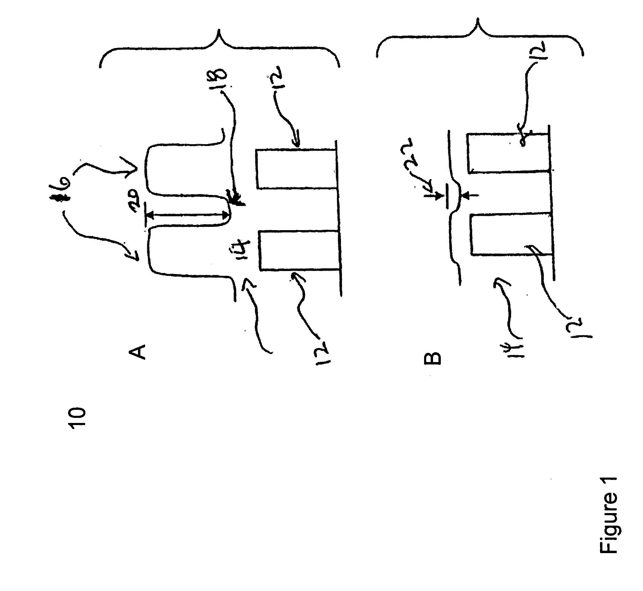
[0217] Customized pad A, designed for polishing oxides, contains a urethane with 70D hardness. Pads are molded using liquid casting and are formulated using methods previously described. Amongst the components a 70D isocyanate, a polyol chain extender, a curative agent, a stabilizer, used for UV protection, and a porosity agent are used for pad manufacture. The pour is carried out at about 150-160° F. After the pour the material is allowed to settle and cure for approximately 15 minutes. Then the pad is removed from the mold and put in an oven for approximately 12 hours for post-cure at a uniform temperature between about 100° F.-200° F. The thickness of the pad is 80 mils and the diameter of the pad is 20 inches. A double side tape is adhered to the backside to get the pad ready for polishing. Customized pad B is similar to customized pad A in terms of formation but the hardness is lower at ˜65D.

[0218] Prestonian plots are presented for the two subject pads described above (FIGS. ...

example 2

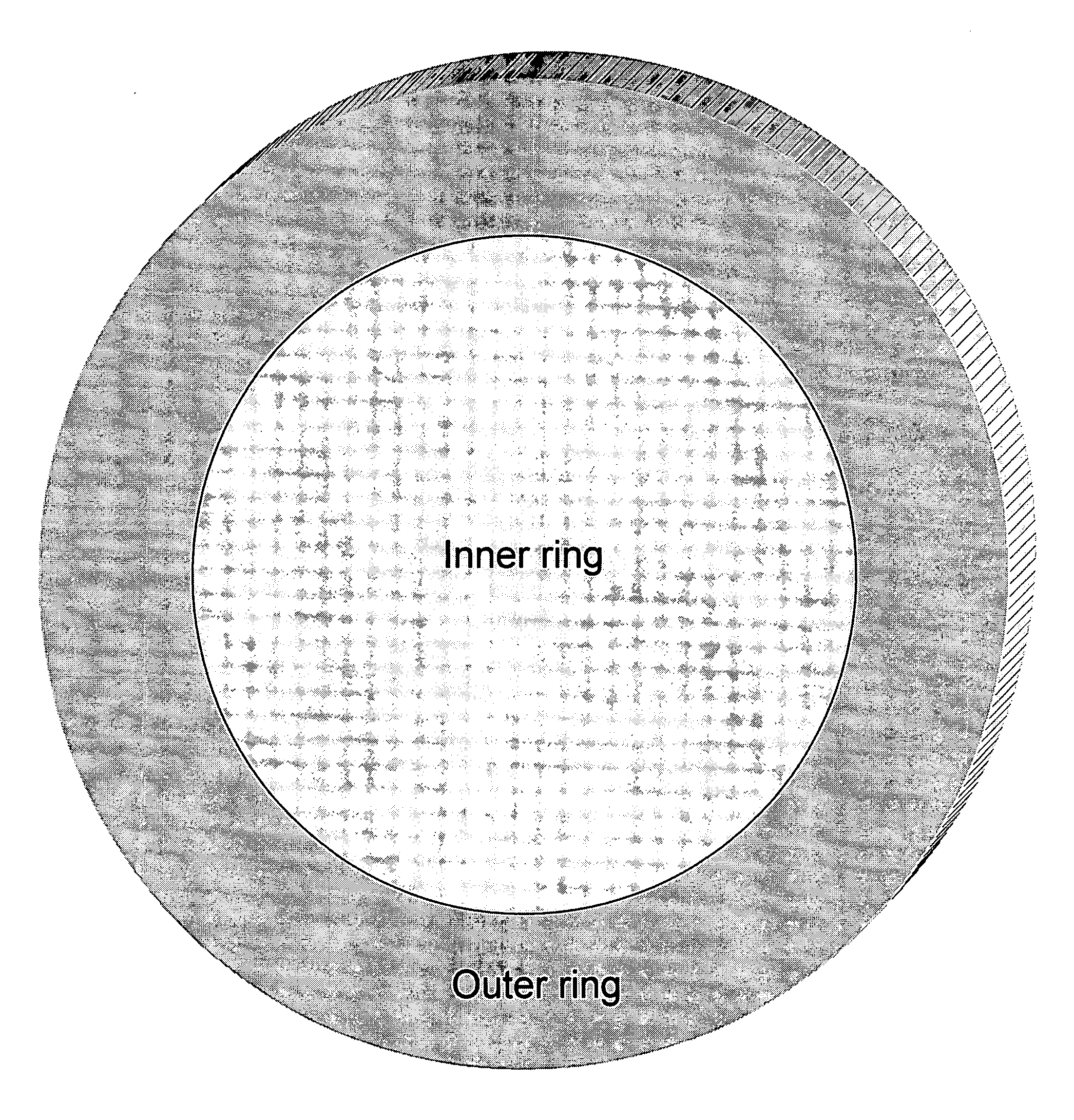
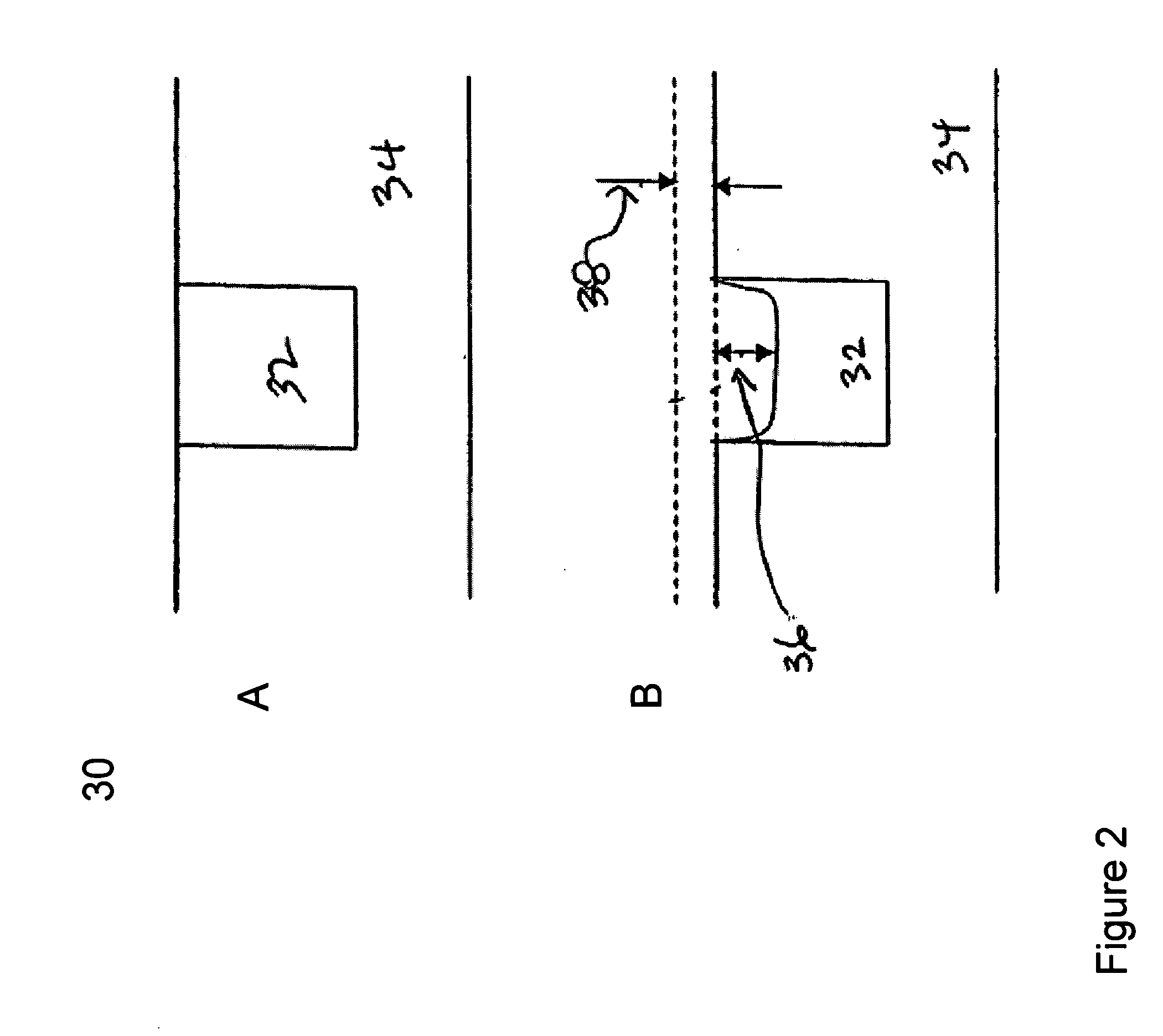
[0220] Pads for polishing oxides are manufactured in a similar fashion as described in example 1. Further, the pads have been functionally graded to improve polishing performance. In FIGS. 28-32 planarization efficiency of Neopad's customized and planarization length comparisons are made using patterned wafers. FIG. 28A shows the die measurement plan where 9 dies are chosen per wafer measurement. FIG. 28 B depicts the structural elements within each of the individual dies. Results are shown in FIGS. 29 and 31, which compares the oxide thickness as a function of the layout pattern density within one dies for three polishing times (30 s, 60 s, and 120 s) for commercial and Neopad's customized pads respectively. The global axis in FIGS. 29 and 31 is for polishing done as a function of pressure and velocity. Die 2 is chosen since it is in the middle of the wafer and sees an effect both from the outer edge of the pad as well as the inner edge of the pad. The slope is approximately 0.5-0....

example 3

[0221] Three pads are fabricated for copper CMP. All three novel pads have a novel micro-structure, are radially graded, can be are sub surface engineered with boron nitride as the solid lubricant, and can be low shear integral pads. (The three novel pads are: 1) a surface engineered pad (novel pad A), 2) a low-shear pad (novel pad B) and 3) a low-shear surface-engineered pad (novel pad C).

[0222] Additionally, copper lines in wafers subjected to the performance testing were analyzed using x-ray diffraction (XRD) and compared to unprocessed wafers to monitor whether or not substantial changes in the copper had occurred, due to stress.

[0223] In FIG. 33 XRD data are displayed. Lattice constant measurements are carried out on wafers polished using each of the five experimental pads (commercial A and B) and novel pads (A, B, and C) and compared to measurements obtained from an unpolished wafer. The lattice constant of the unpolished copper films is 3.6086 Å. The measured lattice consta...


PUM

PropertyMeasurementUnit
Tgaaaaaaaaaa
surface tensionaaaaaaaaaa
sizeaaaaaaaaaa

Abstract

The present application relates to polishing pads for chemical mechanical planarization (CMP) of substrates, and methods of fabrication and use thereof. The pads described in this invention are customized to polishing specifications where specifications include (but not limited to) to the material being polished, chip design and architecture, chip density and pattern density, equipment platform and type of slurry used. These pads can be designed with a specialized polymeric nano-structure with a long or short range order which allows for molecular level tuning achieving superior themo-mechanical characteristics. More particularly, the pads can be designed and fabricated so that there is both uniform and nonuniform spatial distribution of chemical and physical properties within the pads. In addition, these pads can be designed to tune the coefficient of friction by surface engineering, through the addition of solid lubricants, and creating low shear integral pads having multiple layers of polymeric material which form an interface parallel to the polishing surface. The pads can also have controlled porosity, embedded abrasive, novel grooves on the polishing surface, for slurry transport, which are produced in situ, and a transparent region for endpoint detection.

Description

CROSS-REFERENCE TO RELATED APPLICATIONS [0001] This application is a continuation-in-part of U.S. patent application Ser. No. 10 / 810,070, filed on Mar. 25, 2004 which claims the priority benefit of U.S. provisional application No. 60 / 457,273 filed Mar. 25, 2003 and is a continuation-in-part of U.S. patent application Ser. No. 11 / 060,898, filed Feb. 18, 2005 and is a continuation-in-part of PCT application US2004 / 017638, filed Jun. 3, 2004 which claims the priority benefit of U.S. provisional application No. 60 / 457,305, filed Jun. 3, 2003 and is a continuation-in-part of U.S. patent application Ser. No. 10 / 897,192, filed Jul. 21, 2004, the contents of which are herby incorporated by reference into the present disclosure as if fully put forth herein. This application also claims the priority benefit of U.S. provisional patent applications No. 60 / 654,104 filed Feb. 18, 2005, 60 / 654,173, filed Feb. 18, 2005, and 60 / 677,062, filed May 2, 2005 which are herby incorporated by reference int...

Claims


Application Information

Patent Timeline
Patent Type & Authority Applications(United States)
IPC IPC(8): B24B7/30B24D11/00
CPCB24B37/042B24B37/20B24D7/14B24B49/02B24B53/017B24B37/26B33Y10/00
Inventor ROY, PRADIP K.DEOPURA, MANISHMISRA, SUDHANSHU
Owner CMC MATERIALS INC
Why Eureka
Try Eureka