Substrate strip plate structure for semiconductor device and method for manufacturing the same

a technology of semiconductor devices and strip plates, applied in the direction of semiconductor devices, semiconductor/solid-state device details, electrical devices, etc., can solve the problems of destroying the whole device structure, exhibiting significant brittleness during semiconductor device manufacturing, and low yield or product of device manufacturing

Inactive Publication Date: 2014-06-17
SUNOVEL SUZHOU TECH
View PDF0 Cites 3 Cited by
  • Summary
  • Abstract
  • Description
  • Claims
  • Application Information

AI Technical Summary

Benefits of technology

[0056]The present invention makes effective use of the thickness of the substrate, and increases processable surface areas or the utilization rate of surface areas of wafers, on the premise that dimensions of whole wafers are not increased. The present invention proposes to form flexible material layers on surfaces of the strip sheets, therefore, when the upright strip plate array is stretched to form a substantially planar strip plate array with a plurality of connected strip plates, the neighboring strip plates can still be connected through the flexible material layers, even if the strip sheets go ruptured because of their brittleness; therefore, according to the present invention, it becomes quite easy to stretch a plurality of strip plates into a substantially planar array where the strip plates are distributed on a same plane, and to improve efficiency and yield of device structure manufacturing.

Problems solved by technology

Conventional materials like SiO2, SiN exhibit significant brittleness during manufacturing of semiconductor devices.
Therefore, when used to manufacture devices with thin film structure such as solar cells, the materials like SiO2, SiN would rupture easily because of bending or stretching and then cause the connected device structure to break apart, which consequently destroys to the whole device structure or results in low yield or productivity of device manufacturing.

Method used


Image

  • Substrate strip plate structure for semiconductor device and method for manufacturing the same
  • Substrate strip plate structure for semiconductor device and method for manufacturing the same
  • Substrate strip plate structure for semiconductor device and method for manufacturing the same

Examples


Embodiment Construction

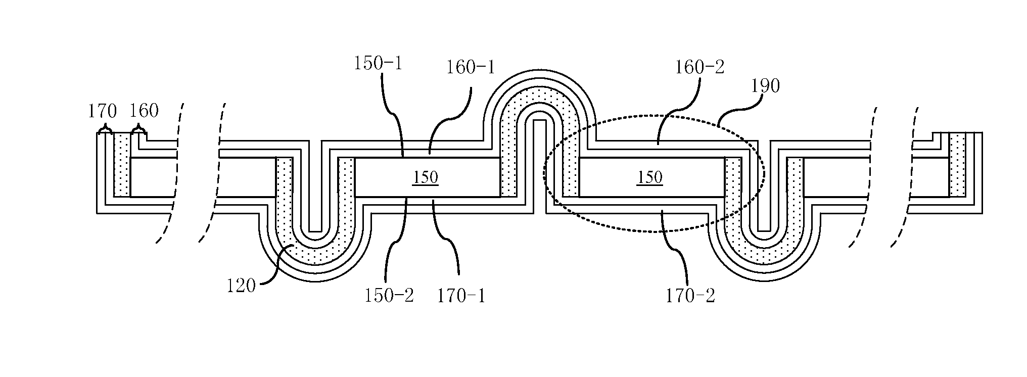
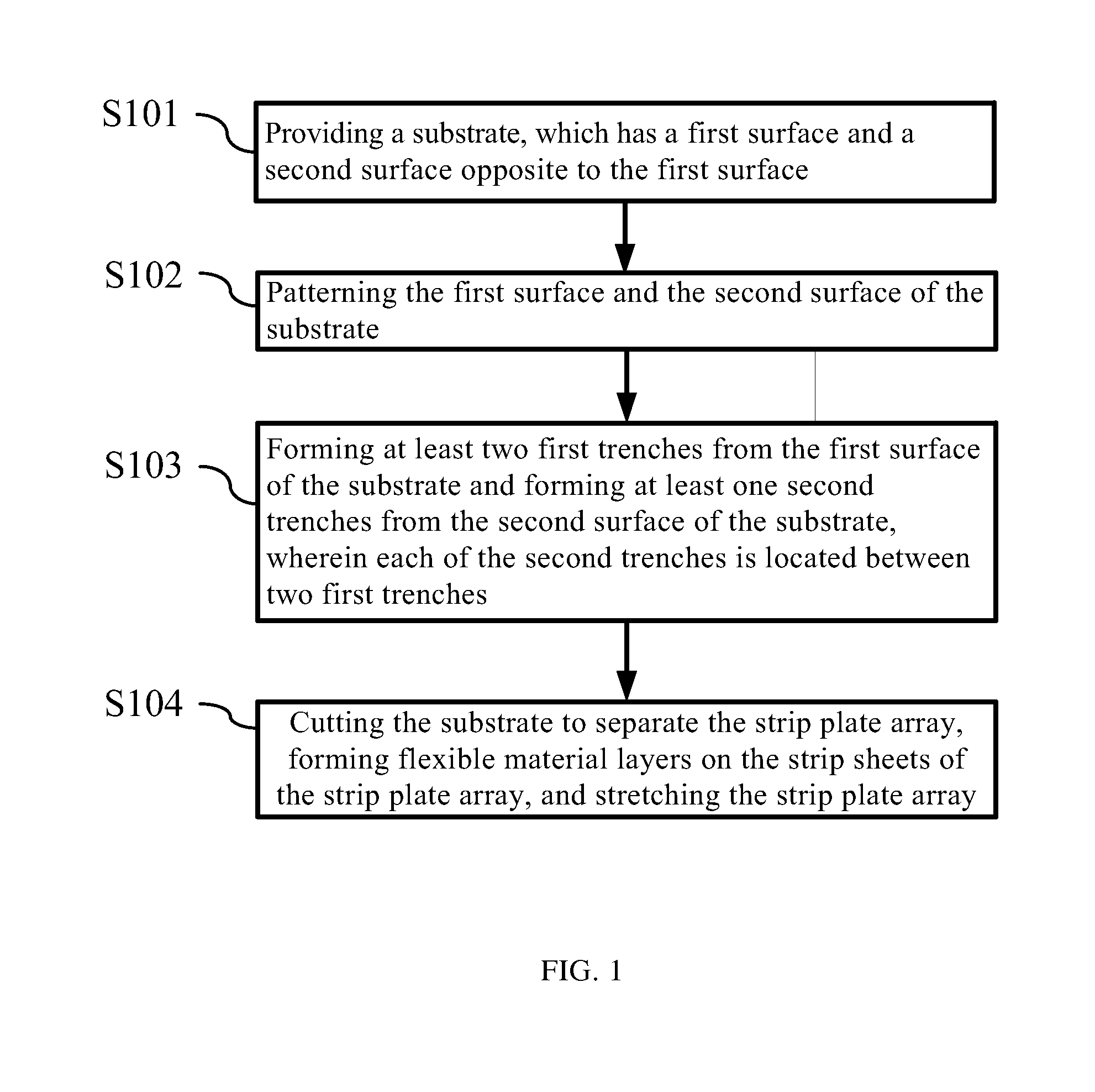
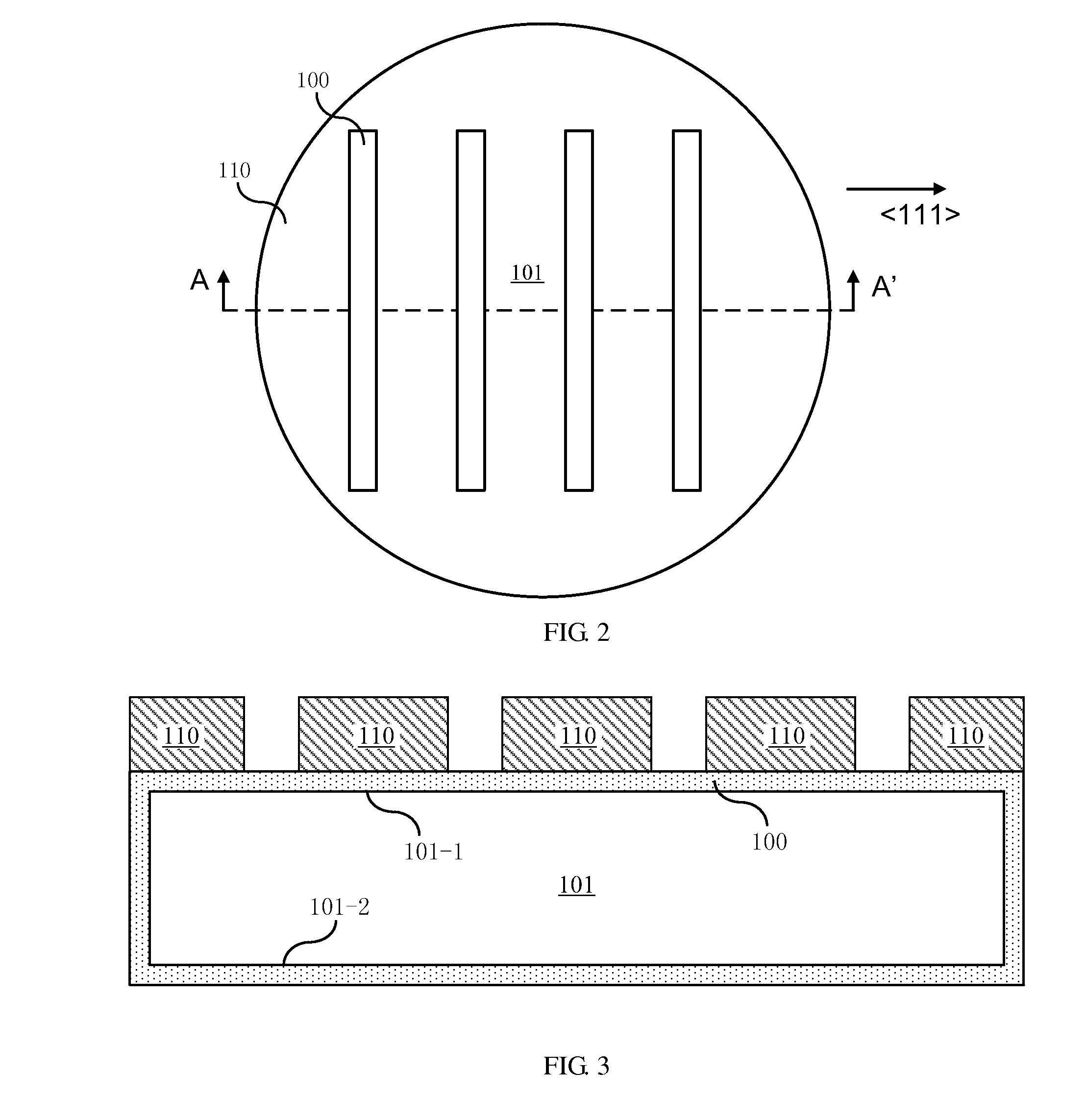
[0062]Embodiments of the present invention are described in detail here below, wherein examples of the embodiments are illustrated in the drawings, in which same or similar reference signs throughout denote same or similar elements or elements have same or similar functions. It should be appreciated that the embodiments described below in conjunction with the drawings are illustrative and are provided for explaining the prevent invention only, thus shall not be interpreted as limitations to the present invention. Various embodiments or examples are provided here below to implement different structures of the present invention. To simplify the disclosure of the present invention, description of components and arrangements of specific examples is given below. Of course, they are illustrative only and not limiting the present invention. Moreover, in the present invention, reference numbers and / or letters may be repeated in different embodiments. Such repetition is for purposes of simpl...


PUM


Abstract

The present invention provides a strip plate structure and a method for manufacturing the same. The strip plate structure comprises a strip plate array, which comprises a plurality of strip plates arranged with spacing in a predetermined direction on a same plane, wherein each of the strip plates has a first surface and a second surface opposite to the first surface and the strip plate array is arranged on a plane parallel to the first surface of the strip plates; a plurality of strip sheets which connect neighboring ones of the strip plates; flexible material layers, which are located on at least a portion of the surfaces of the strip sheets and / or on at least a portion of the surfaces of the strip plates.

Description

[0001]This application claims priority to U.S. application No. 61 / 212,673 filed on Apr. 15, 2009, U.S. application Ser. No. 13 / 264,063 filed on Oct. 12, 2011, Chinese patent application 201110025831.0 filed on Jan. 24, 2011, PCT application PCT / CN2012 / 070534 filed on Jan. 18, 2012. All of the U.S. applications, PCT patent application and Chinese patent application are incorporated herein by reference in their entireties.FIELD OF THE INVENTION[0002]The present invention relates to the field of semiconductor manufacturing, particularly, to a strip plate structure with an increased surface area for semiconductor device manufacturing and a method for manufacturing the same.BACKGROUND OF THE INVENTION[0003]In recent years, with rapid development in the semiconductor industry, development of semiconductor devices is oriented towards a trend of smaller dimension, higher circuit density, faster operation speed and lower power consumption; integrated circuits have entered a technical phase o...

Claims


Application Information

Patent Timeline
Patent Type & Authority Patents(United States)
IPC IPC(8): H01L23/52H01L21/768
CPCH01L27/1218
Inventor ZHU, HUILONGLUO, ZHIJIONGYIN, HAIZHOU
Owner SUNOVEL SUZHOU TECH
Why Eureka
Try Eureka