Light source device and display device

a technology of light source and display device, which is applied in the direction of lighting and heating apparatus, semiconductor devices for light sources, instruments, etc., can solve the problems of color unevenness, color unevenness, and easy deterioration of the phosphor layer, so as to suppress the generation of color unevenness and suppress the fluctuation of intensity

Active Publication Date: 2014-07-08
DEXERIALS CORP
View PDF14 Cites 20 Cited by
  • Summary
  • Abstract
  • Description
  • Claims
  • Application Information

AI Technical Summary

Benefits of technology

[0009]However, in the direct-under type light source device using the white point source of light described above, a phosphor should be applied on a surface of a tiny LED chip, which is approximately 1 mm or less in size. Therefore, there has been a problem that variation in application (unevenness in thickness) of the phosphor layer is generated among units, and thereby color unevenness occurs easily. Also, the phosphor layer easily deteriorates depending on the environment in each package, which has also been a factor of causing the color unevenness.
[0010]The present invention has been made in view of the above-described problem, and an object of the invention is to provide a light source device capable of suppressing generation of color unevenness, and a display device using the same.
[0015]According to the light source device and the display device of the present invention, the color conversion layer, which converts part of each color light in one wavelength region emitted from the light emitting section into the color light in another wavelength region, is provided to be spaced apart from the light emitting section and opposed to the light emitting section, in the light source device. This makes it possible to suppress the fluctuation of intensity in each color light as compared with a configuration in which a color conversion layer is formed adjacent to an excitement light source. Therefore, it is possible to suppress generation of color unevenness.

Problems solved by technology

Therefore, there has been a problem that variation in application (unevenness in thickness) of the phosphor layer is generated among units, and thereby color unevenness occurs easily.
Also, the phosphor layer easily deteriorates depending on the environment in each package, which has also been a factor of causing the color unevenness.

Method used


Image

  • Light source device and display device
  • Light source device and display device
  • Light source device and display device

Examples


first embodiment

[0033][First Embodiment]

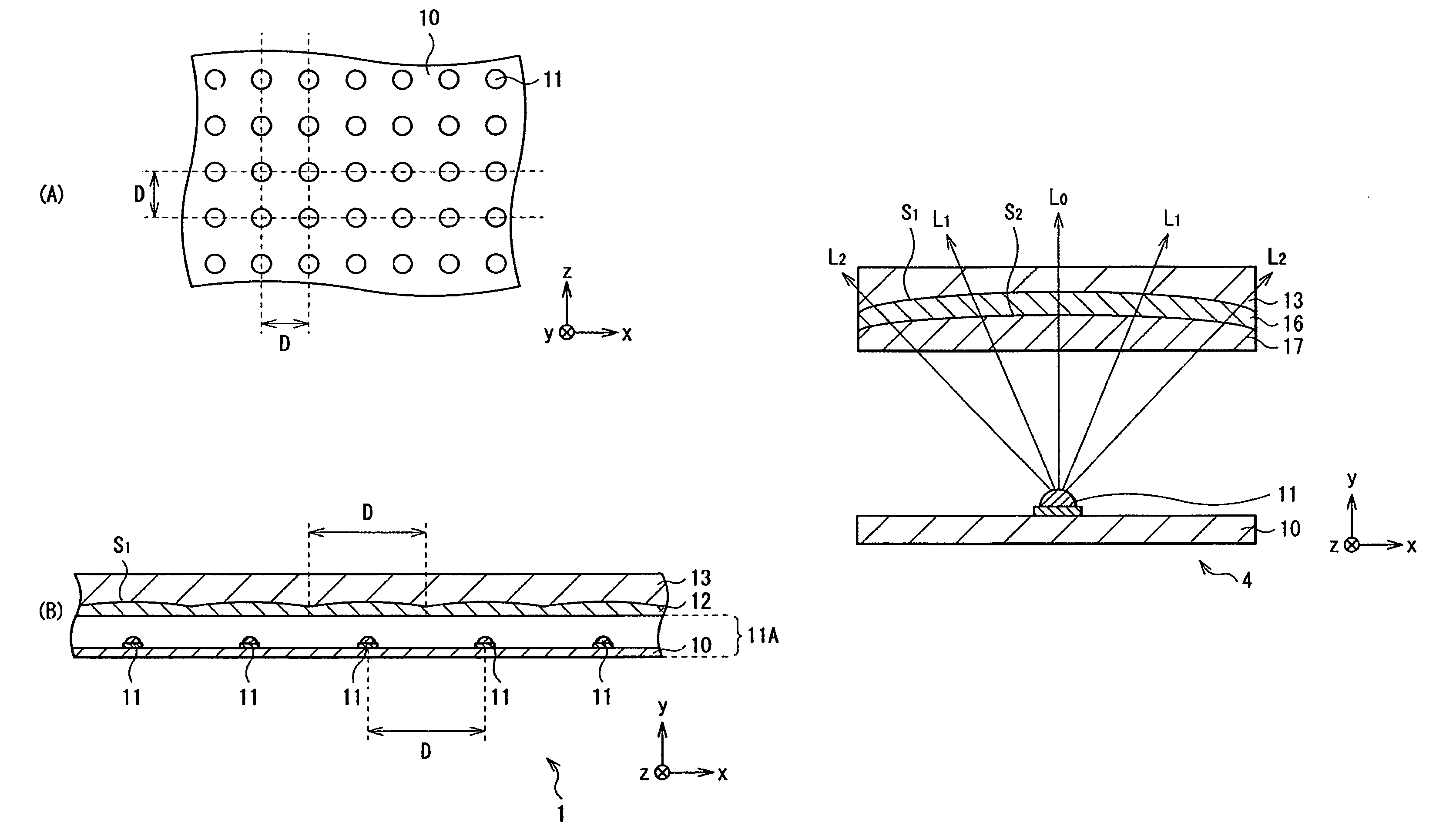
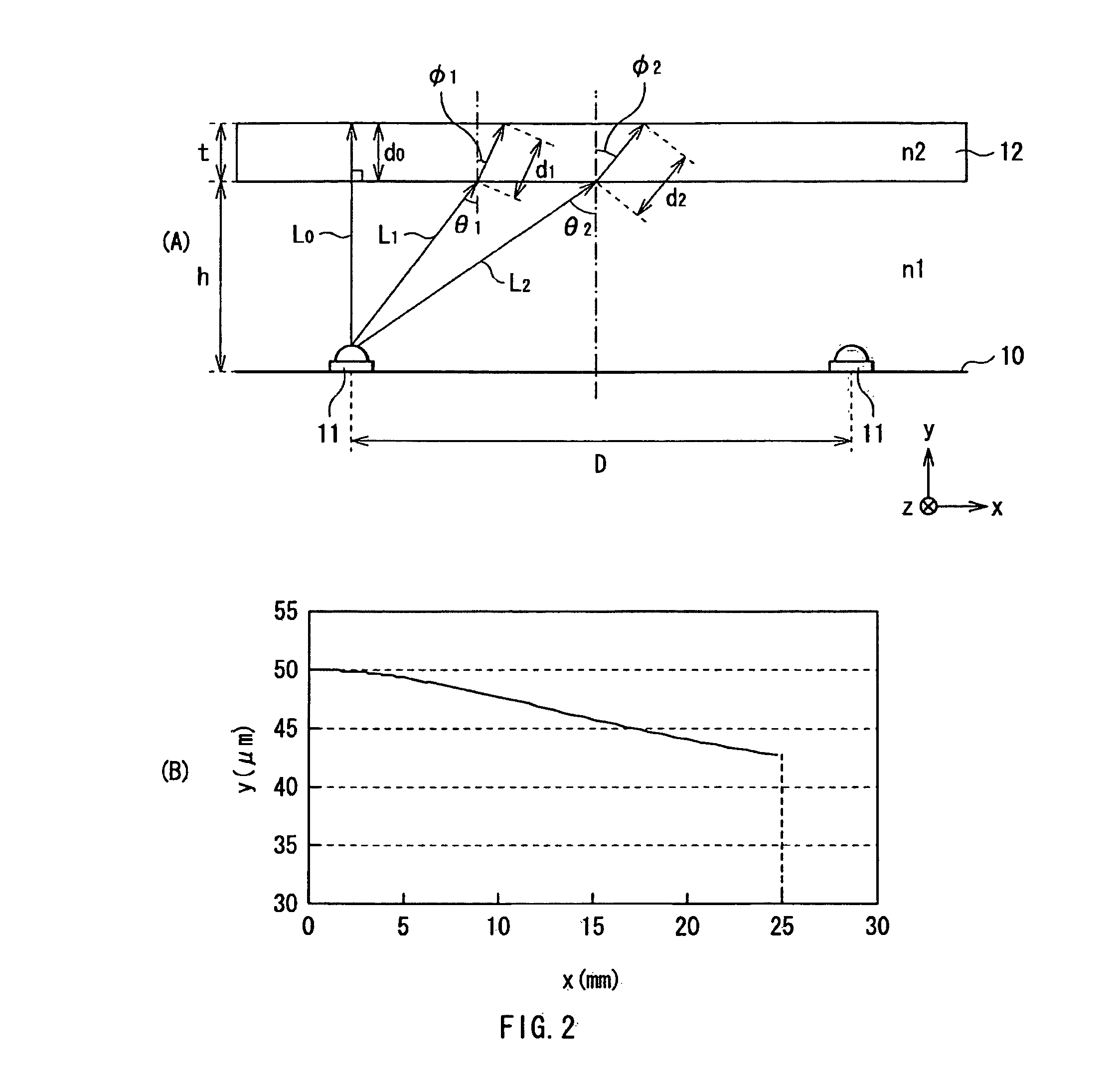
[0034]FIG. 1(A) is a z-x plan view illustrating a schematic configuration of a light source device (hereinafter referred to as a light source device 1) according to a first embodiment of the invention, and FIG. 1(B) is an x-y sectional view thereof. The light source device 1 is arranged with a plurality of excitement light sources within the same plane, and thereby performs surface light-emission as a whole. This light source device 1 is provided with a phosphor layer (color conversion layer) 12 and a diffusion layer 13, which are sequentially arranged in this order above a light emitting section 11A. The light emitting section 11A is arranged with a plurality of excitement light sources (point sources of light) 11, which are arranged on a substrate 10 at predetermined intervals D. Incidentally, each of the first embodiment to a third embodiment to be described below is a configuration example in which the plurality of point sources of light are arranged on t...

modification 1

[0054](Modification 1)

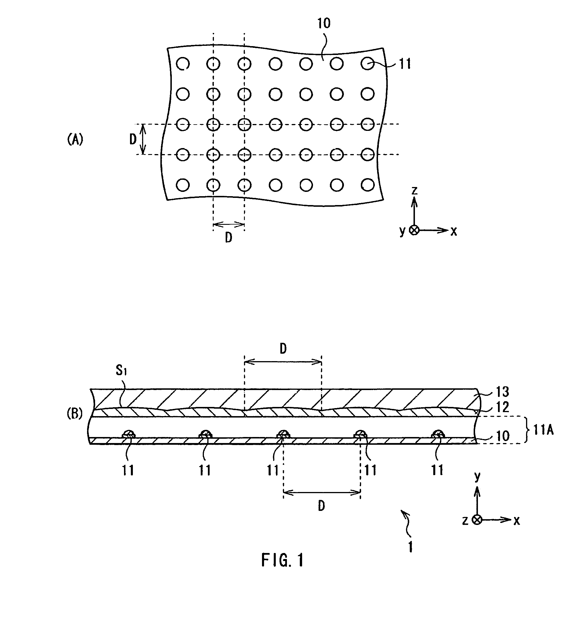
[0055]FIG. 6 is a sectional view illustrating a schematic configuration of a light source device 4 according to Modification 1 of the present embodiment. In the light source device 4, a configuration is similar to that of the light source device 1 described above, except that a light incident surface of a phosphor layer 16 has a curved surface S2 which is concave on the light incident side (hereinafter simply referred to as a concave curved surface), and a base film (transparent substrate) 17 is provided adjacent to the concave curved surface S2. However, the light source device 4 is configured such that a light path length within the phosphor layer 16 becomes uniform by a combination of the convex curved surface S1 and the concave curved surface S2.

[0056]The phosphor layer 16 can be formed, for example, as follows. First, as described above, the base film 17 is prepared separately from the diffusion layer 13 previously formed with the concave-convex shape whic...

modification 2

[0058](Modification 2)

[0059]FIG. 7 is a sectional view illustrating a schematic configuration of a light source device 5 according to Modification 2 of the present embodiment. In the light source device 5, a configuration is similar to that of the light source device 1 described above, except that a light incident surface of a phosphor layer 18 has a curved surface S3 which is convex on the light incident side (hereinafter simply referred to as convex curved surface), and a base film 19 is provided adjacent to the curved surface S3. Also, it has the configuration similar to that of the Modification 1 described above, except that a surface on the light incident side of the phosphor layer 18 has the convex curved surface S3. A curved surface shape thereof can be formed with a procedure similar to that of the Modification 1. Accordingly, even with the configuration in which the convex curved surface S1 is formed on the light exit surface of the phosphor layer 18 and the convex curved s...


PUM


Abstract

A light source device capable of suppressing generation of color unevenness, and a display device using the same are provided. The light source device 1 is provided with a plurality of excitation light sources 11 which are arranged at prescribed intervals D on a substrate 10 and emit blue light, and a phosphor layer 12 which converts part of the blue light emitted from the excitation light sources into red light and green light and arranged at a distance from the excitation light sources 11 to oppose the substrate 10. Fluctuation of intensity of each color light due to nonuniform application of the phosphor layer is difficult to occur as compared with a configuration in the past where the phosphor layer is formed adjacent to each excitation light source.

Description

TECHNICAL FIELD[0001]The present invention relates to a light source device used as a backlight of a liquid crystal display device for example, and to a display device using the same.[0002]The present application is based on and claims priority from Japanese Patent Application No. 2007-316688 and No. 2008-140900, filed in Japan on Dec. 7, 2007 and May 29, 2008 respectively, the disclosures of which are hereby incorporated by reference.BACKGROUND ART[0003]In the past, there have been proposed various light source devices as backlights of liquid crystal display (LCD: Liquid Crystal Display) devices, which are used in liquid crystal display televisions, laptop personal computers, car navigation systems, etc. (for example, see Patent Documents 1 to 3). Each of the light sources described in these Patent Documents employs an edge light method utilizing a light guiding means. However, reduction in thickness and increase in area of the liquid crystal display devices are in progress in rece...

Claims


Application Information

Patent Timeline
Patent Type & Authority Patents(United States)
IPC IPC(8): F21V9/00F21V9/16
CPCF21K9/00G02F1/133617G02F2001/133607G02F2001/133614G02F1/133603G02F1/133609G02F1/133607G02F1/133614
Inventor YOSHIDA, TETSUYUKIMASUDA, SHOZONADA, NAOJIITO, YASUSHITSUKAHARA, TSUBASA
Owner DEXERIALS CORP
Why Eureka
Try Eureka