
Light source device for an image forming apparatus

a technology of light source device and image forming apparatus, which is applied in the direction of lighting and heating apparatus, instruments, optical elements, etc., can solve the problems of increasing cost, limiting the accuracy of positioning, and limiting the range of light source devices, etc., to achieve high accuracy and low cost

Inactive Publication Date: 2001-01-30
RICOH KK
View PDF9 Cites 15 Cited by
  • Summary
  • Abstract
  • Description
  • Claims
  • Application Information

AI Technical Summary

Benefits of technology

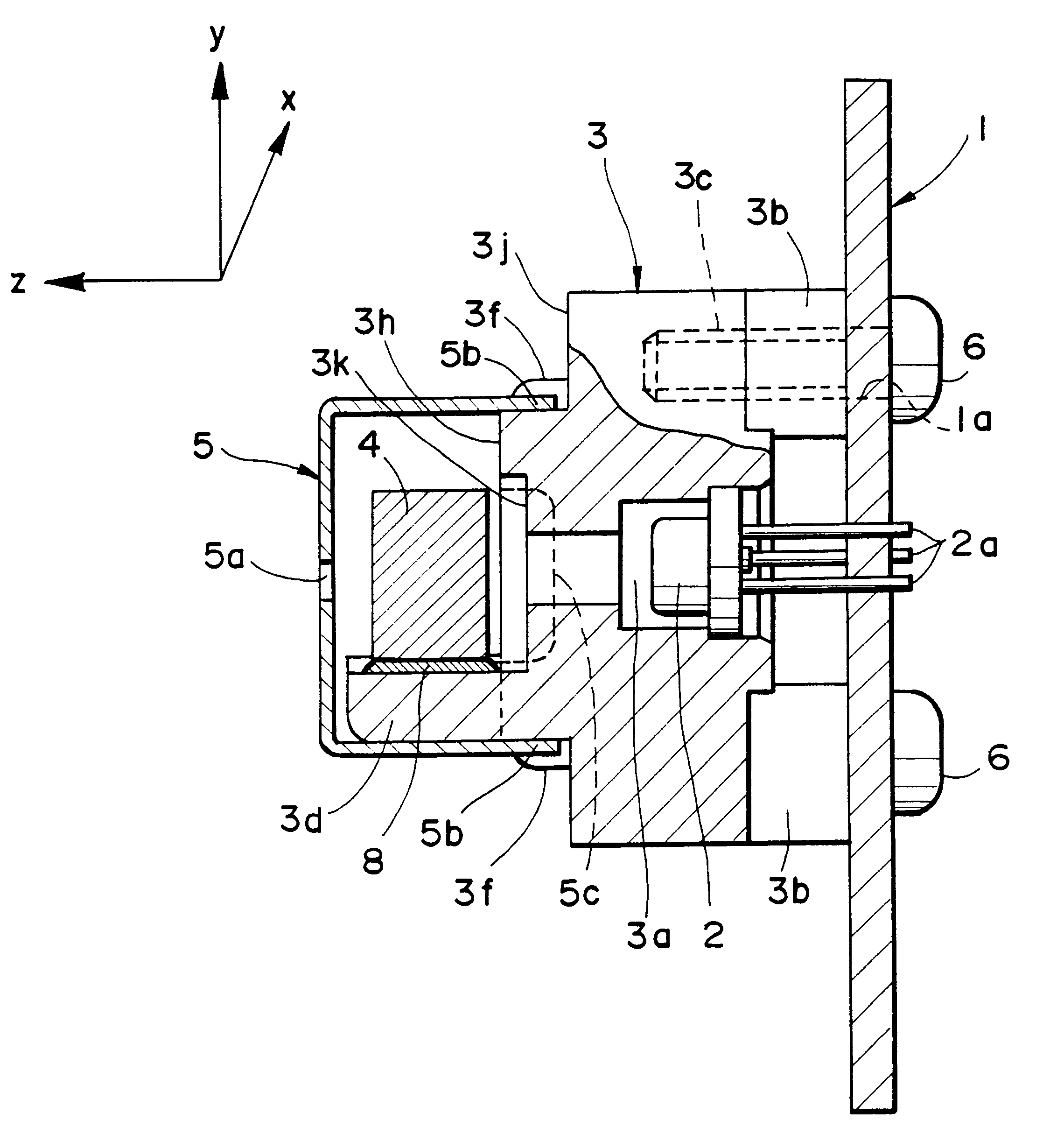
It is therefore an object of the present invention to provide an inexpensive and highly accurate light source device needing a minimum number of constituent parts, protecting the individual part from dislocation during assembly, and allowing a collimator lens to be fixed in place by photo-curable adhesive.
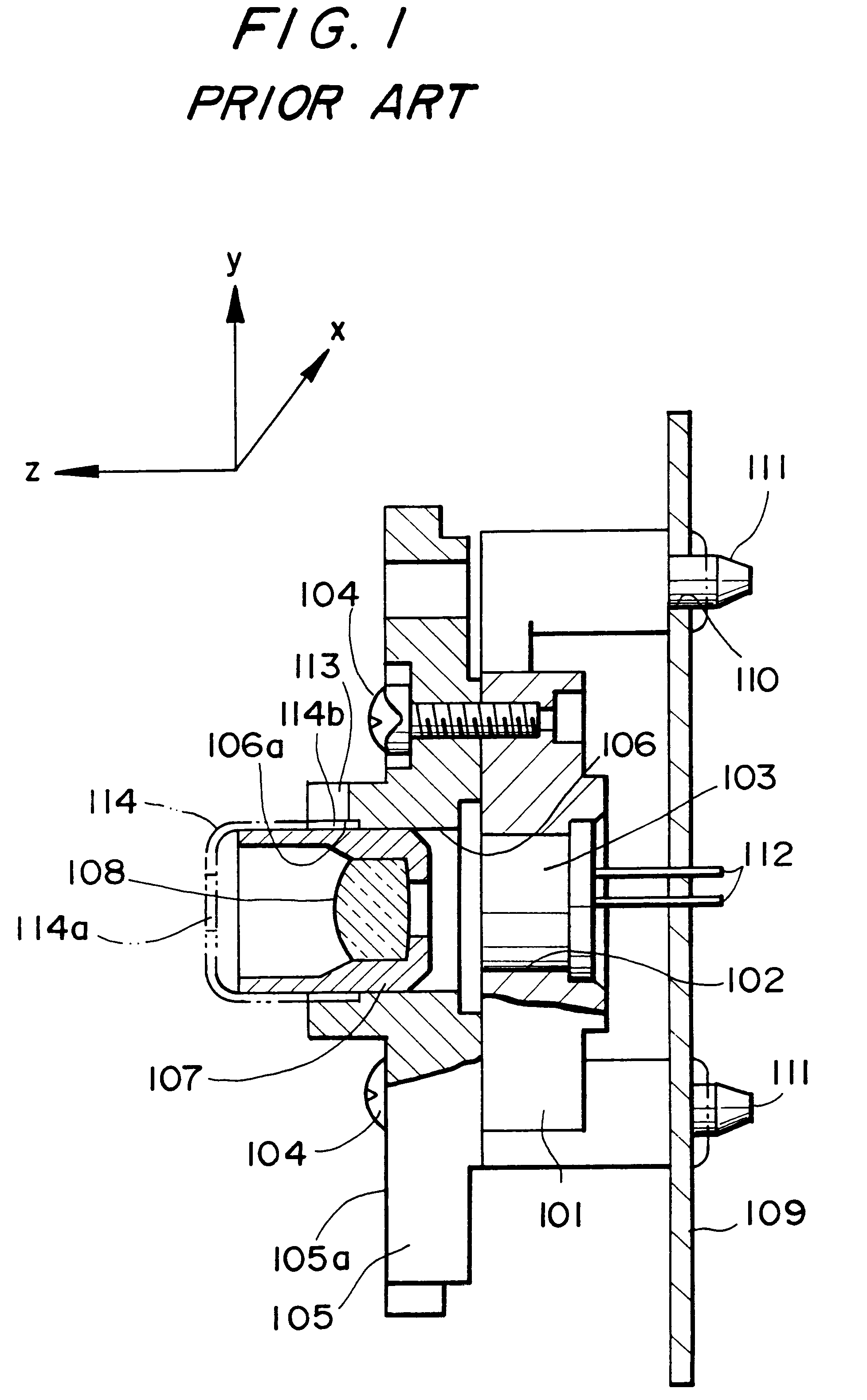
(12) The laser 103 is easily deteriorated or damaged by static electricity or similar electrical noise. Ideally therefore, the device should be assembled and adjusted fully automatically so as to be isolated from static electricity issuing from the human body. The automatic assembly and adjustment will save labor cost and will improve quality and yield of products. In an automatic machine, the reference surface for setting workpieces including light source devices should advantageously be horizontal, considering the loading and unloading of the workpieces.. When the production of the light source device having the reference surface 105a perpendicular to the optical axis is automat it should preferably be set down (causing the laser beam to issue downward) in order to facilitate the production. However, such a configuration requires the adhesive to be introduced into the assembly downward or sideways after the adjustment of the collimator lens 108. This is not practical, considering the drop of the adhesive Moreover, the aperture must be mounted to the assembly from below the assembly after the injection of the adhesive, complicating the automatic machine or requiring an extra step.

Problems solved by technology

The positional accuracy is severely restricted to below the order of microns.
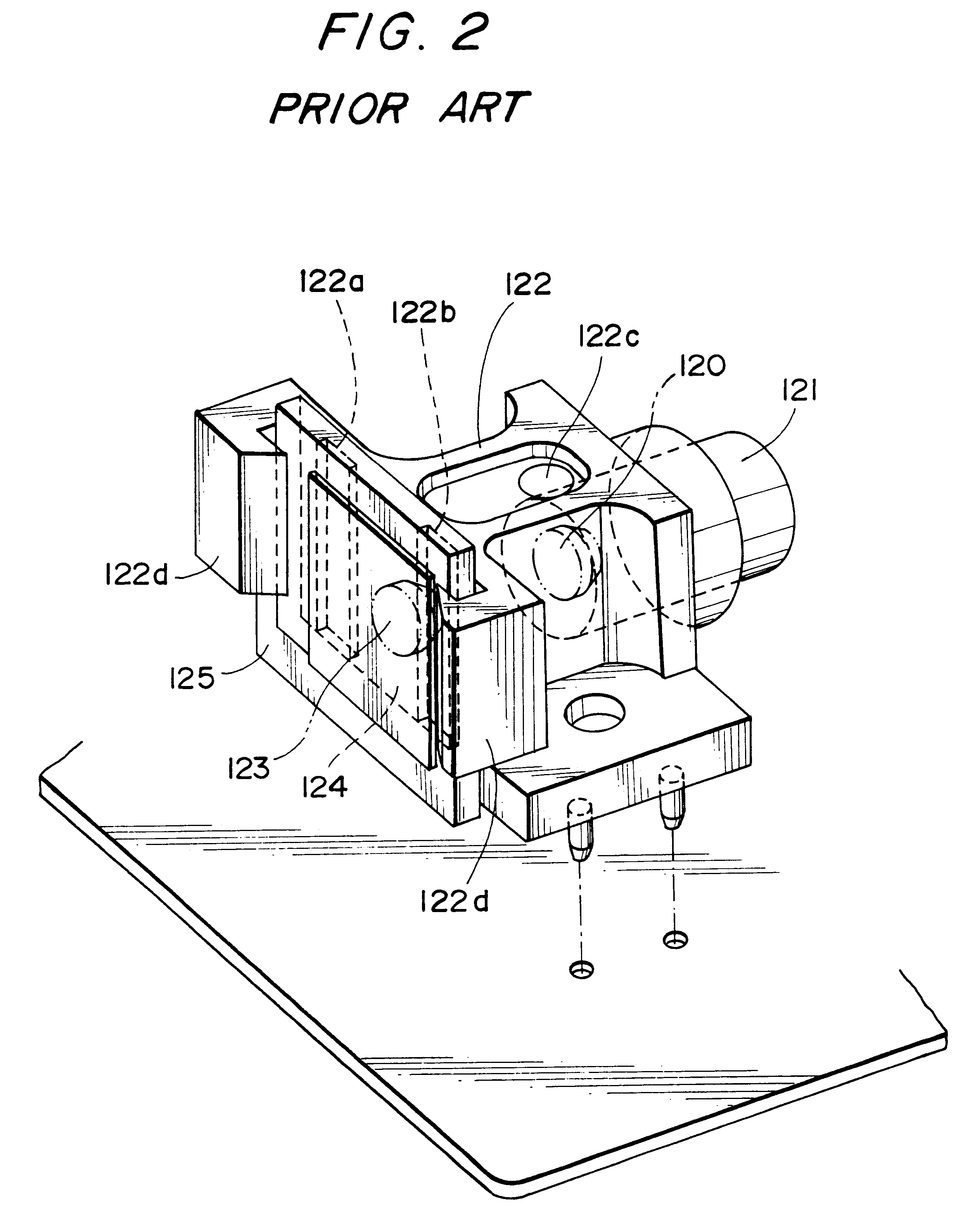
However, the conventional devices of the type described have some problems yet to be solved, as follows:
(1) Each device needs a number of constituent parts which increase the cost.
(3) Use cannot be made of ultraviolet light curable adhesive for fixing the collimator lens in place.
The conventional devices have other problems which will be described, in addition to the above problems.

Method used


Image

  • Light source device for an image forming apparatus
  • Light source device for an image forming apparatus
  • Light source device for an image forming apparatus

Examples


2nd embodiment

Referring to FIG. 14, an alternative embodiment of the present invention will be described. As shown, the light source device has a base or support member 15 formed with a stepped through bore 16 substantially at its center. A semiconductor laser 12 is press fitted in the bore 16. The base 15 is formed of a substance opaque to infrared rays (about 780 nm) and light having shorter wavelengths. The base 15 has on its outer surface a first cylindrical surface 18 and a second cylindrical surface 17 smaller in diameter than the first cylindrical surface 18. A guide pin 11 protruding from the right end of the base 15, as viewed in FIG. 14, is passed through a positioning hole 10a formed in a printed circuit board 10, and then affixed to the circuit board 10 by thermal deformation. The laser 12 and circuit board 10 are electrically connected together by leads 12a.

A collimator leas 19 is formed of a material transparent to ultraviolet rays, While the lens 19 may be implemented as a plastic ...

3rd embodiment

FIGS. 15 and 16 show another alternative embodiment of the present invention In FIGS. 15 and 16, structural elements identical with the elements shown in FIG. 14 are designated by identical reference numerals. As shown, the light source device has a base or support member 23 formed of the same material as the base 15, FIG. 14. The semiconductor laser 12 is press fitted in the through bore 16 formed in the base 23. The guide pin 11 protruding from the right end of the base 23 is received in the hole 10a of the printed circuit board 10 and then deformed by heat. As a result, the circuit board 10 is affixed to the base 23. The aperture forming member 14 is press fitted on the cylindrical surface 18 of the base 23. The configuration described so far is identical with the configuration shown in FIG. 14.

In this embodiment, the smaller diameter cylindrical surface 17 is replaced with a recessed surface 24 contiguous with the greater diameter cylindrical surface 18. A cylindrical collimator...

4th embodiment

Referring to FIGS. 17 and 18, a further alternative embodiment of the present invention will be described. As shown, the light source device has a semiconductor laser 33 for emitting laser light, a collimator lens 38 for collimating the laser light to output a substantially parallel beam, and a base or support member 35 supporting the laser 33. The base 35 is formed of a material opaque to light having wavelengths shorter than about 780 mm (infrared rays) inclusive.

The laser 33 is press fitted in a stepped through bore 35a formed in substantially the center of the base 35. A pair of spacers 35b are formed integrally with the base 35. Guide pins 35c each protrudes from the respective spacer 35b. A printed circuit board 30 is formed with positioning holes 30a slightly smaller in diameter the guide pins 35c. The base 35 is affixed to the circuit board 30 with its guide pins 35 received in the positioning holes 30a. After the base 35 has been affixed to the circuit board 30, leads 33a e...


PUM


Abstract

A light source device for use in an image forming apparatus and using a semiconductor laser is disclosed. The device needs a minimum of constituent parts and frees the individual part from dislocation in the event of assembly. A collimator lens included in the device is fixed in place by photo-curable adhesive. The device is low cost and highly accurate.

Description

The present invention relates to a light source device for use in an image forming apparatus and using a semiconductor laser.A digital copier, laser printer, facsimile apparatus or similar image forming apparatus extensively used today includes a light source device having a semiconductor laser and collimator leas. Optical characteristics required of the light source device include the directivity of laser light (optical axis characteristic) and the parallelism of a beam (collimation characteristic). To meet these requirements, it is a common practice to adjust the relative position of the emission point of the laser and the collimator lens in the directions of three axes (x, y and z). The positional accuracy is severely restricted to below the order of microns. Therefore, the device using the laser and collimator lens must be capable of being adjusted in the three axis directions and then fixed at its adjusted position.When the collimator lens is fixed in place by adhesive, the adh...

Claims


Application Information

Patent Timeline
Patent Type & Authority Patents(United States)
IPC IPC(8): G02B6/42
CPCG02B6/4204G02B6/4239B41J2/471
Inventor NAOE, YASUHIROYASHIBA, AKIOYAMANAKA, HIDEYASU
Owner RICOH KK
Learn More