

Optical-semiconductor encapsulating material
a technology of optical shielding and encapsulation material, which is applied in the direction of semiconductor devices, semiconductor/solid-state device details, electrical devices, etc., can solve the problems of easy deterioration of resin, increase of fluorescent material-containing resin portion, etc., and achieve the effect of convenient us
- Summary
- Abstract
- Description
- Claims
- Application Information
AI Technical Summary
Benefits of technology
Problems solved by technology
Method used
Image

Examples
example 1
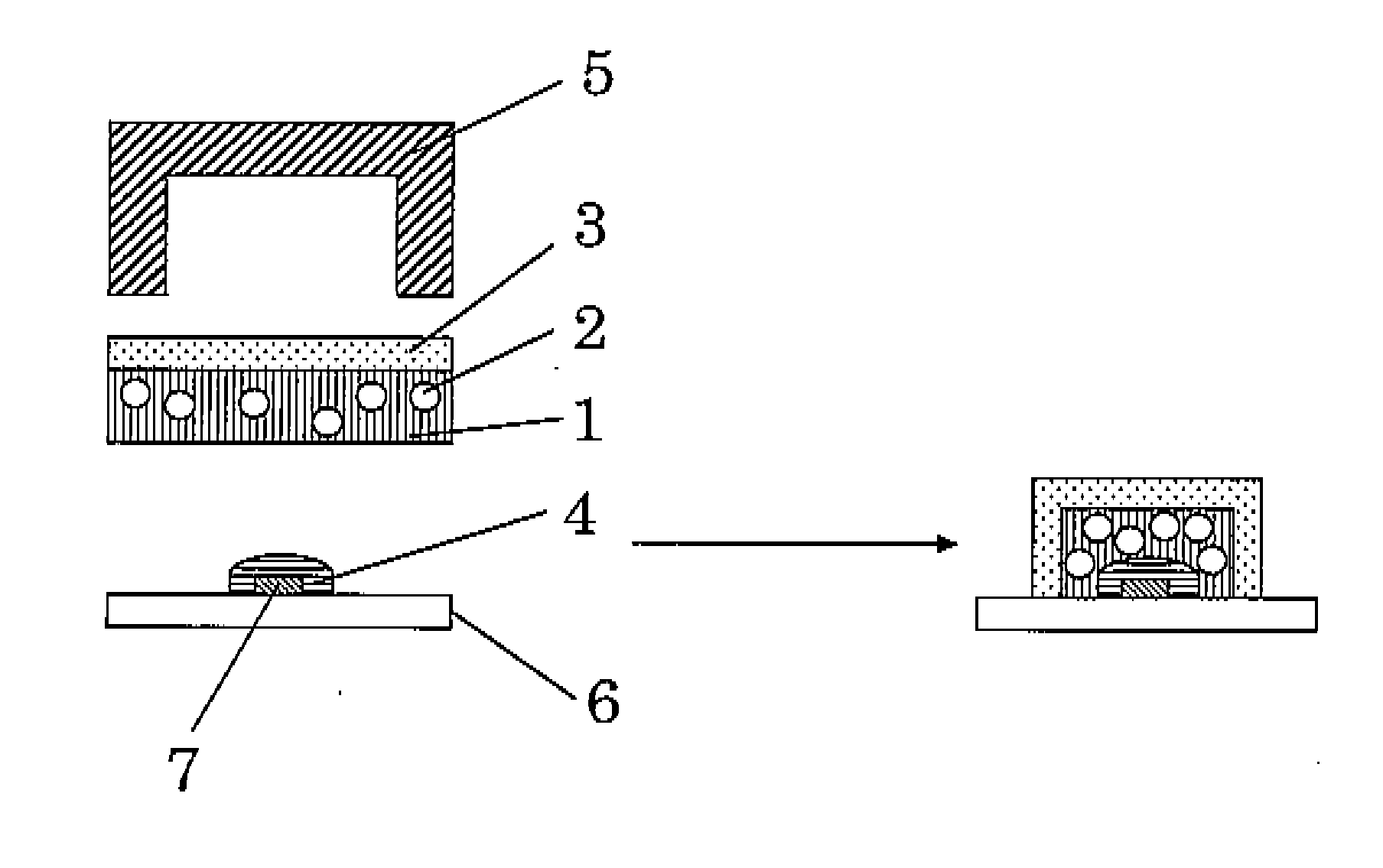
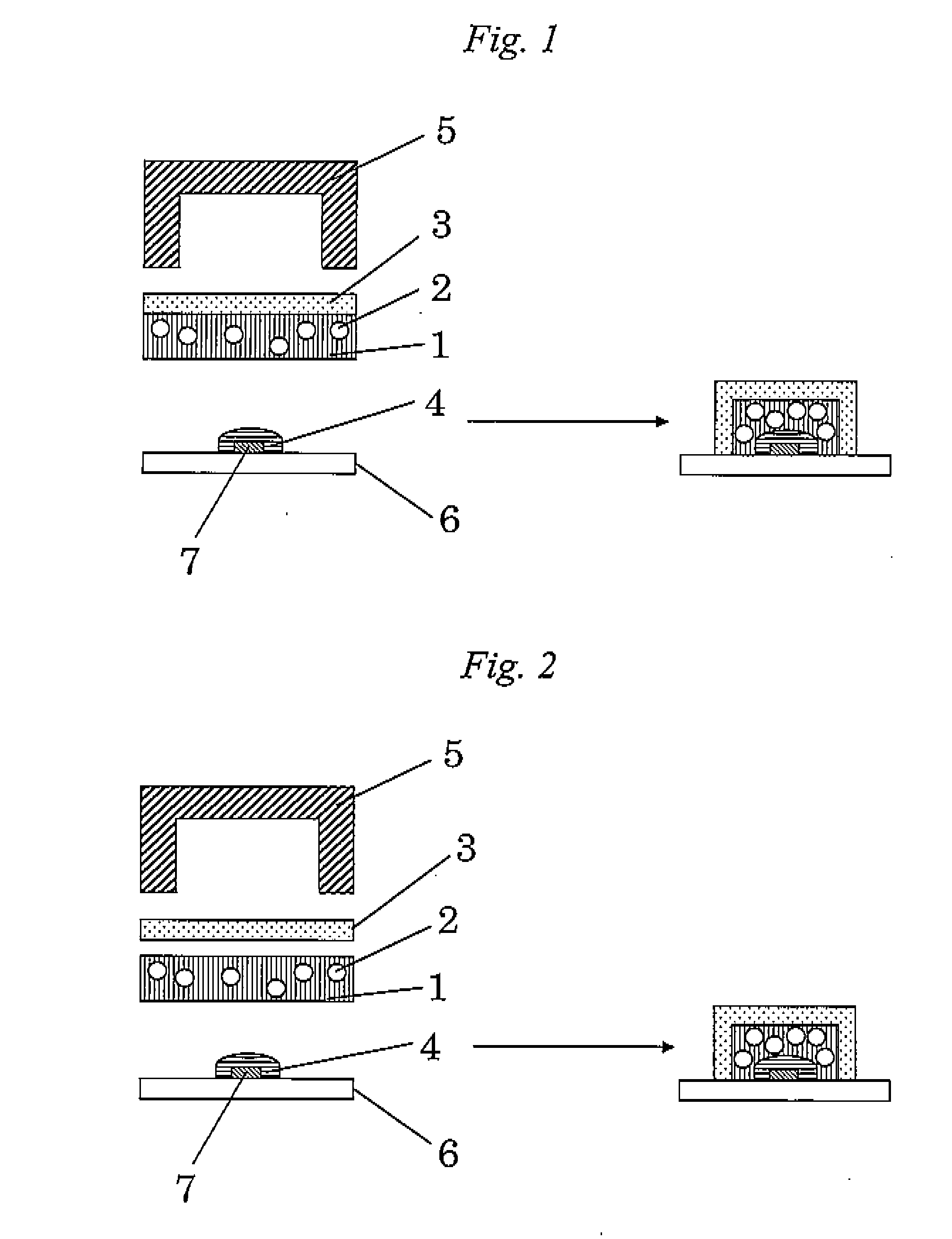
First Resin Layer
[0066]To 9.95 g of a silicone elastomer (ELASTOSIL LR-7665, manufactured by Wacker Asahikasei Silicone Co., Ltd.) was added 0.05 g of silicon dioxide (FB-7SDC, manufactured by Denki Kagaku Kogyo K.K.; average particle size: 5.8 μm; spherical) (content of inorganic particles, 0.5% by weight). The silicon dioxide was uniformly dispersed by hand stirring to obtain a liquid silicon dioxide-containing resin.
Second Resin Layer
[0067]To 8.4 g of a silicone elastomer (LR-7665) was added 1.6 g of YAG (content of phosphor: 16% by weight). The YAG was uniformly dispersed by hand stirring to obtain a liquid phosphor-containing resin.
[0068]The phosphor-containing resin was applied with an applicator to a polycarbonate film in a thickness of 100 μm and dried at 90° C. for 4 minutes and 30 seconds to obtain a phosphor-containing resin sheet. The silicon-dioxide-containing resin was likewise applied on the resultant phosphor-containing resin sheet in a thickness of 500 μm and dried ...
example 2
[0070]An optical semiconductor device was obtained in the same manner as in Example 1, except that the amounts of the silicone elastomer (LR-7665) and the silicon dioxide (FB-7SDC) in the first resin layer were changed to 9.5 g and 0.5 g, respectively (content of inorganic particles, 5% by weight).
example 3
[0071]An optical semiconductor device was obtained in the same manner as in Example 1, except that the amounts of the silicone elastomer (LR-7665) and the silicon dioxide (FB-7SDC) in the first resin layer were changed to 7.0 g and 3.0 g, respectively (content of inorganic particles, 30% by weight).
PUM
 Abstract
Description
Claims
Application Information