
Substrate processing method

a substrate and processing method technology, applied in the direction of instruments, cleaning using liquids, other chemical processes, etc., can solve the problems of pattern collapse, substrate surface may not be hydrophobic enough, pattern collapse cannot be prevented, etc., to shorten the processing time of substrates.

Active Publication Date: 2014-09-02
DAINIPPON SCREEN MTG CO LTD
View PDF58 Cites 7 Cited by
  • Summary
  • Abstract
  • Description
  • Claims
  • Application Information

AI Technical Summary

Benefits of technology

The present invention relates to a substrate processing method and apparatus for suppressing pattern collapse during semiconductor device fabrication. The invention includes the steps of holding a substrate, supplying a first hydrophobizing agent to the substrate to make its surface hydrophobic, supplying a second hydrophobizing agent to further enhance the hydrophobicity of the substrate surface, and drying the substrate. The substrate processing apparatus includes a substrate holding unit, a first hydrophobizing agent supply unit, a second hydrophobizing agent supply unit, a drying unit, and a controller for controlling these units. The substrate processing method and apparatus can help to prevent pattern collapse during semiconductor device fabrication.

Problems solved by technology

However, pattern collapse cannot be prevented if the surface of the substrate is not sufficiently hydrophobized.
That is, in a case where the surface of the substrate is only partially hydrophobized or in a case where a contact angle of a processing liquid with respect to the substrate is not sufficiently large, pattern collapse cannot be prevented even if the substrate is dried after being hydrophobized.
When, as in the substrate processing method described in U.S. Patent Application Publication No. 2010 / 0240219 A1, a single type of hydrophobizing agent is supplied to the substrate, the surface of the substrate may not be hydrophobized sufficiently.
Also, when a surface tension of the processing liquid adhering to the substrate is high, a large force is applied to the pattern during drying of the substrate.
However, the surface tension of pure water is high and thus even if the substrate is hydrophobized, pattern collapse cannot be prevented sufficiently.
Meanwhile, even when a silylating agent is supplied as a hydrophobizing agent to a substrate having a metal film formed thereon, the metal film is not hydrophobized and thus the substrate cannot be hydrophobized sufficiently.
However, research by the present inventor has shown that even when a metal hydrophobizing agent is used, there are cases where the substrate cannot be hydrophobized sufficiently.
Specifically, a metal hydrophobizing agent is not stable by itself and another solvent (diluting solvent) must be mixed with the metal hydrophobizing agent.
That is, in a case where a solvent containing a hydroxyl group is mixed with the metal hydrophobizing agent or in a case where the metal hydrophobizing agent is supplied to a substrate holding a solvent containing a hydroxyl group, the metal hydrophobizing agent cannot exhibits its ability sufficiently.

Method used


Image

  • Substrate processing method
  • Substrate processing method
  • Substrate processing method

Examples


first embodiment

[First Embodiment]

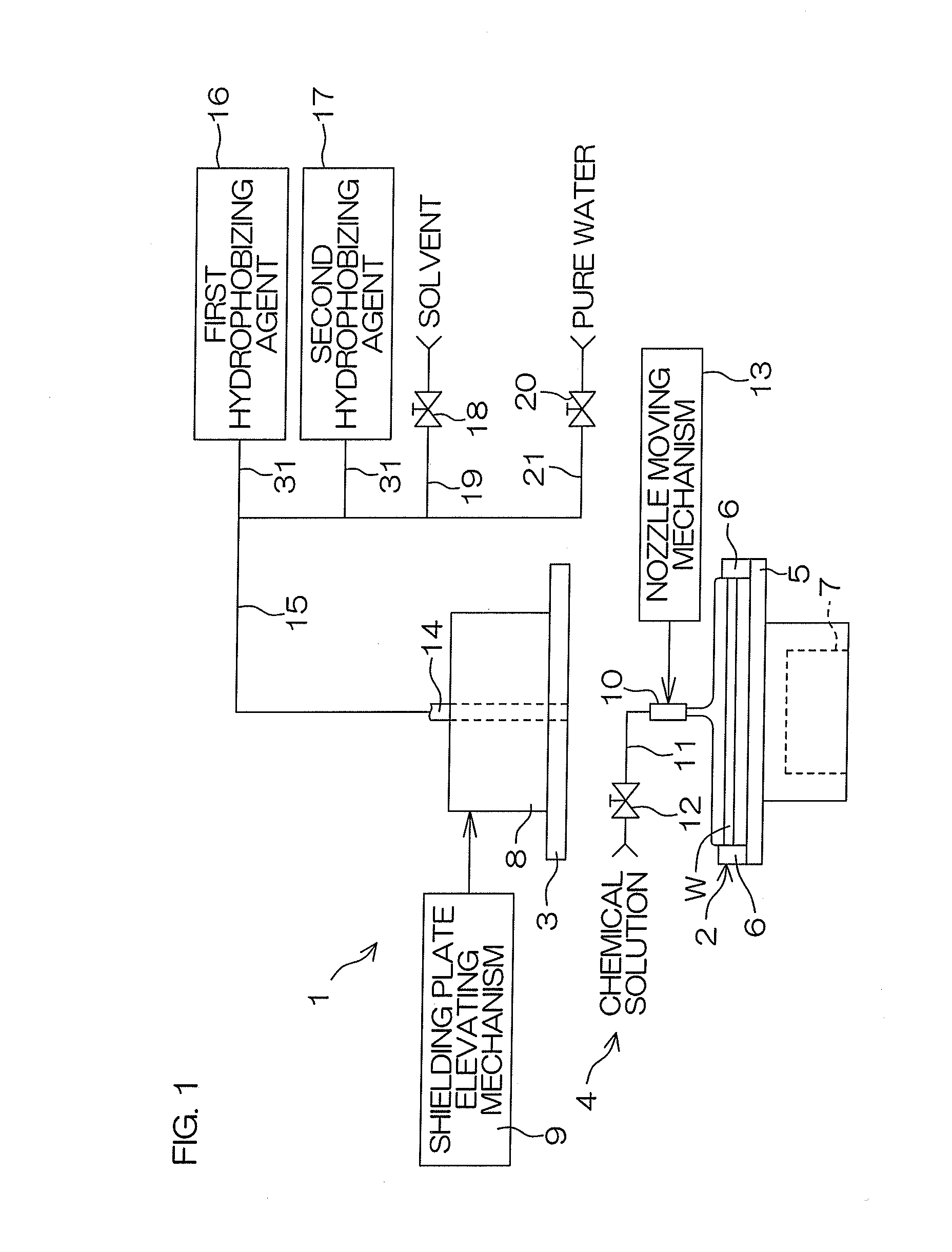
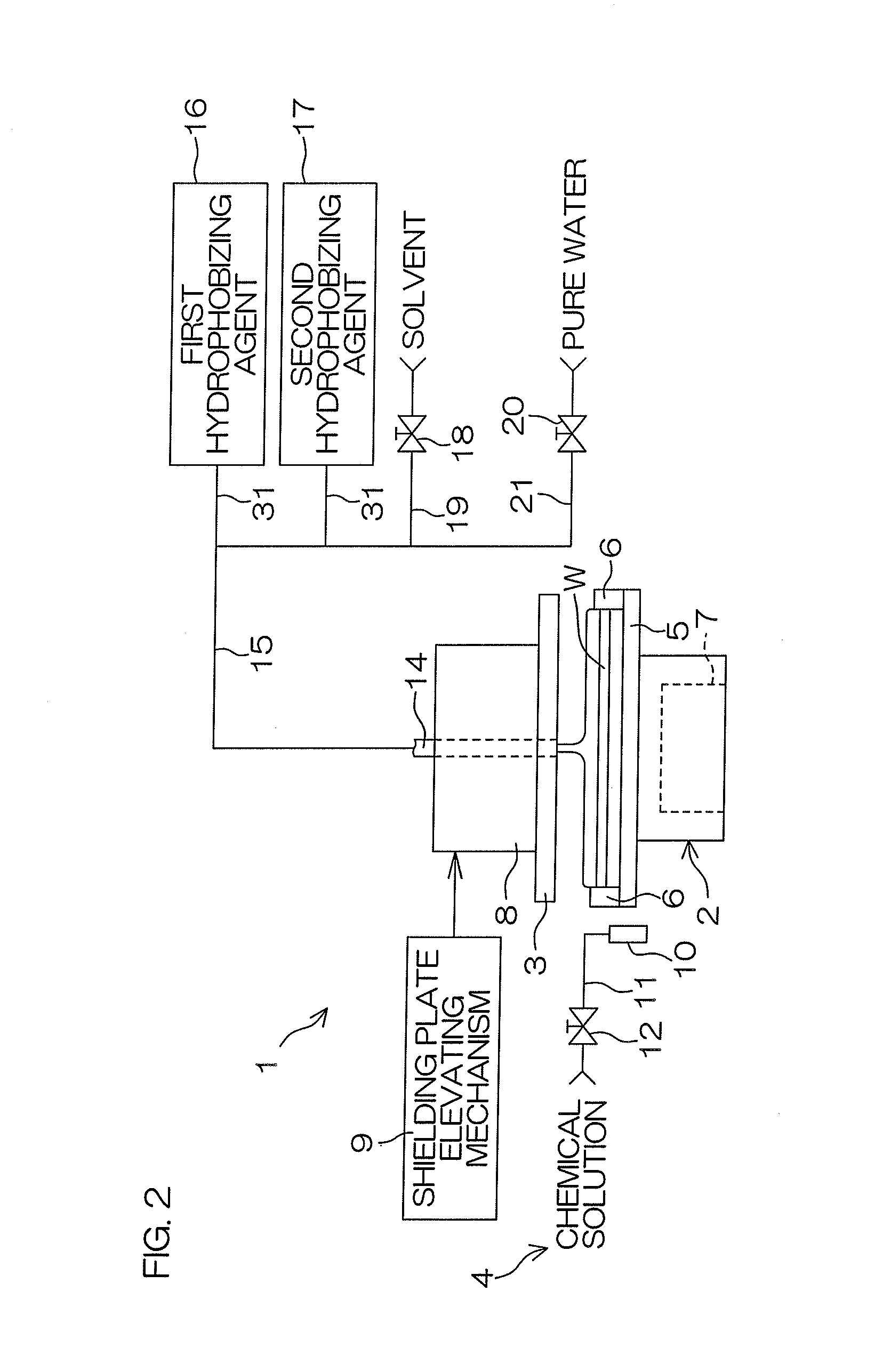
[0099]Each of FIG. 1 and FIG. 2 is a schematic view of a general arrangement of a substrate processing apparatus 1 according to a first embodiment of the present invention. FIG. 3 is a block diagram for describing an electrical arrangement of the substrate processing apparatus 1 according to the first embodiment of the present invention.

[0100]The substrate processing apparatus 1 is a single substrate processing type substrate processing apparatus that processes a semiconductor wafer or other substrate W one at a time by a chemical solution, a rinsing liquid, and other processing liquids. As shown in FIG. 1 and FIG. 2, the substrate processing apparatus 1 includes a spin chuck 2 (substrate holding unit, drying unit) that horizontally holds and rotates the substrate W, a shielding plate 3 disposed above the spin chuck 2, and a processing liquid supply mechanism 4 that supplies the processing liquids to the substrate W held by the spin chuck 2.

[0101]The spin chuck 2 i...

second embodiment

[Second Embodiment]

[0189]FIG. 17 is a schematic view of a general arrangement of a substrate processing apparatus 201 according to a second embodiment of the present invention. FIG. 18 is a schematic view of a general arrangement of a first hydrophobizing agent supply unit 216 according to the second embodiment of the present invention. In FIG. 17 and FIG. 18, component portions that are equivalent to the respective portions shown in FIG. 1 to FIG. 16 described above are provided with the same reference symbols as in FIG. 1, etc., and description thereof shall be omitted.

[0190]A main point of difference of the second embodiment with respect to the first embodiment is that the substrate processing apparatus 201 includes the first hydrophobizing agent supply unit 216 (hydrophobizing agent supply unit, first hydrophobizing agent supply unit) and a second hydrophobizing agent supply unit 217 (hydrophobizing agent supply unit, second hydrophobizing agent supply unit) that supply a vapor ...

third embodiment

[Third Embodiment]

[0207]FIG. 21 and FIG. 22 are schematic views of a general arrangement of a substrate processing apparatus 301 according to a third embodiment of the present invention, with each figure showing a different state.

[0208]The substrate processing apparatus 301 is a single substrate processing type substrate processing apparatus that processes a semiconductor wafer or other substrate W one at a time by a chemical solution, a rinsing liquid, and other processing liquids. The substrate processing apparatus 301 includes a spin chuck 302 (substrate holding unit) that horizontally holds and rotates the substrate W, a shielding plate 303 disposed above the spin chuck 302, and a processing liquid supply mechanism that supplies the processing liquids to the substrate W held by the spin chuck 302.

[0209]The spin chuck 302 is, for example, a gripping type chuck that grips and holds the substrate W. The spin chuck 302 includes, for example, a disk-shaped spin base 304 that is dispo...


PUM

PropertyMeasurementUnit
contact angleaaaaaaaaaa

Abstract

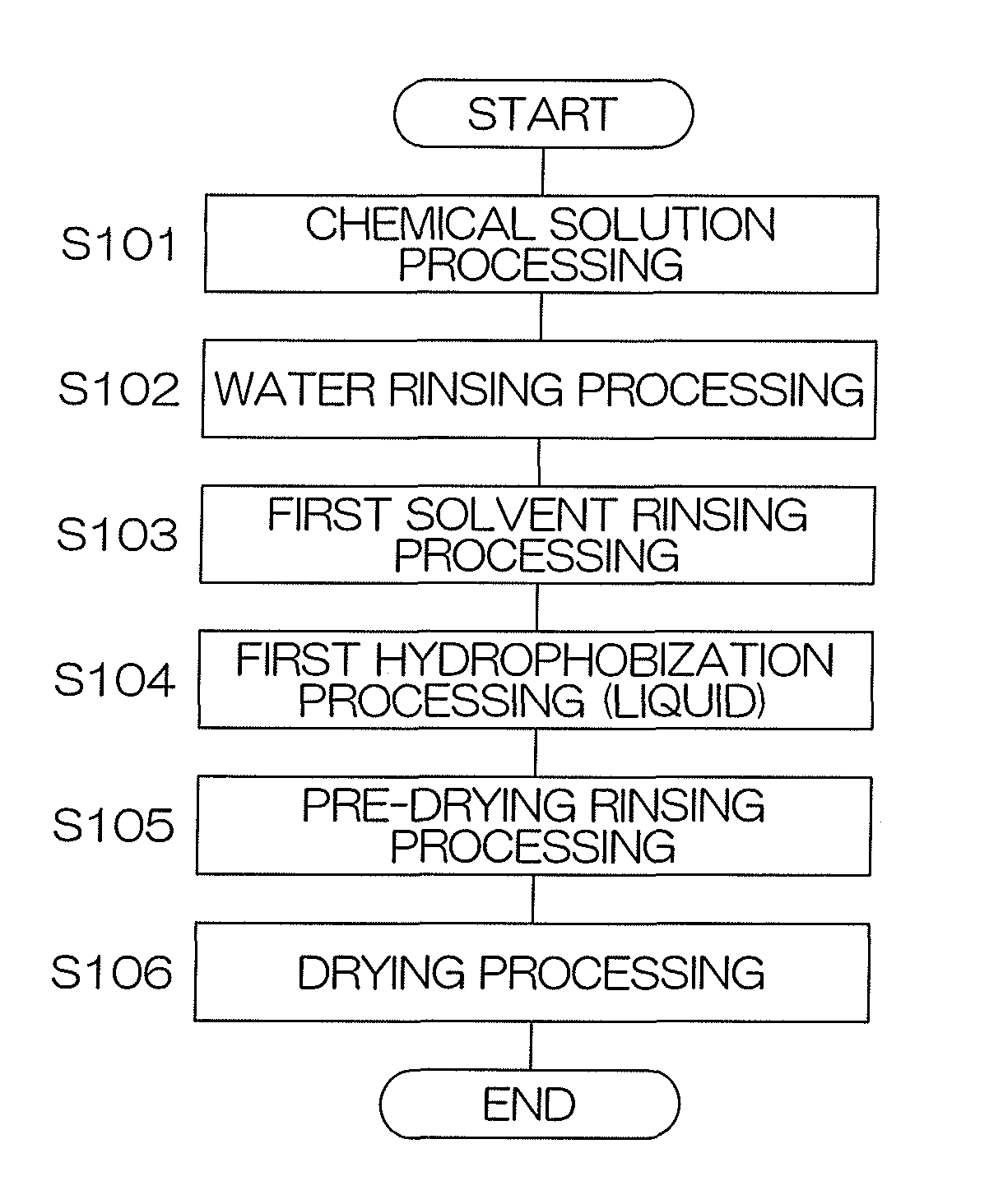
A liquid hydrophobizing agent is supplied to a substrate and a surface of the substrate is hydrophobized. A solvent, lower in surface tension than water and capable of dissolving the hydrophobizing agent, is supplied to the substrate in a pre-drying rinsing step. Thereafter, the substrate is dried. The substrate to be processed is maintained in a state of not contacting water until it is dried after being hydrophobized.

Description

BACKGROUND OF THE INVENTION[0001]1. Field of the Invention[0002]This invention relates to a substrate processing method and a substrate processing apparatus for processing a substrate. Examples of substrates to be processed include semiconductor wafers, substrates for liquid crystal displays, substrates for plasma displays, substrates for FEDs (Field Emission Displays), substrates for optical disks, substrates for magnetic disks, substrates for magneto-optical disks, substrates for photomasks, ceramic substrates, and substrates for solar cells.[0003]2. Description of Related Art[0004]In a production process for a semiconductor device or a liquid crystal display, a substrate, such as a semiconductor wafer or a glass substrate for a liquid crystal display, is processed, for example, one by one. Specifically, a chemical solution is supplied to the substrate and a surface of the substrate is processed by the chemical solution. Thereafter, pure water is supplied and the chemical solution...

Claims


Application Information

Patent Timeline
Patent Type & Authority Patents(United States)
IPC IPC(8): B05D3/02C23C16/00
CPCH01L21/02068H05K3/227H01L21/67051H01L21/321B08B3/08H01L21/3105H01L21/306H01L21/6708H01L21/02057F26B1/00H01L21/67028B05D3/002B05D3/007C09K3/185C23C26/00G03F1/60G03F7/2041G03F7/70916H01L21/0274
Inventor KIMURA, MASAHIROKOJIMARU, TOMONORIEMOTO, TETSUYAOKUTANI, MANABUOTSUJI, MASAYUKI
Owner DAINIPPON SCREEN MTG CO LTD
Learn More