

Substrate processing method and substrate processing apparatus
a substrate and processing method technology, applied in the direction of instruments, cleaning using liquids, other chemical processes, etc., can solve the problems of pattern collapse, substrate surface may not be hydrophobic enough, pattern collapse cannot be prevented, etc., to shorten the processing time of substrates.
- Summary
- Abstract
- Description
- Claims
- Application Information
AI Technical Summary
Benefits of technology
Problems solved by technology
Method used
Image

Examples
first embodiment
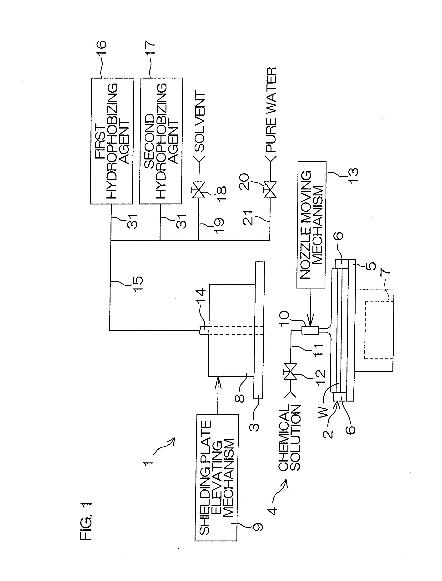
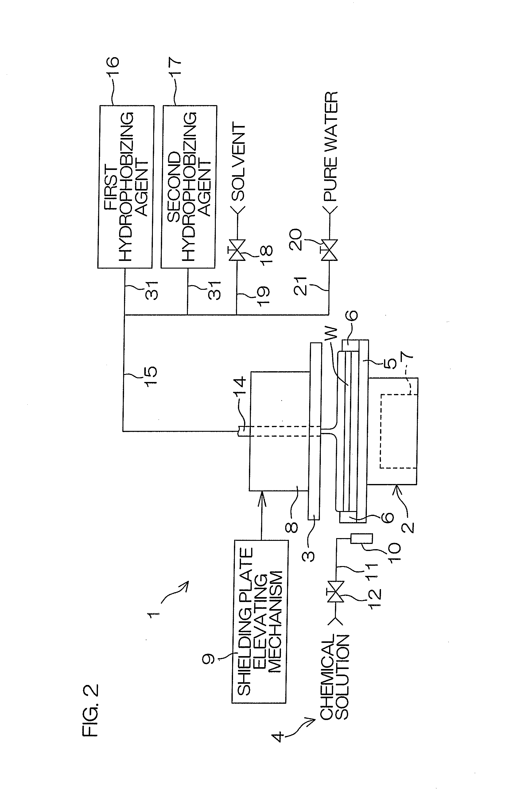
[0099]Each of FIG. 1 and FIG. 2 is a schematic view of a general arrangement of a substrate processing apparatus 1 according to a first embodiment of the present invention. FIG. 3 is a block diagram for describing an electrical arrangement of the substrate processing apparatus 1 according to the first embodiment of the present invention.
[0100]The substrate processing apparatus 1 is a single substrate processing type substrate processing apparatus that processes a semiconductor wafer or other substrate W one at a time by a chemical solution, a rinsing liquid, and other processing liquids. As shown in FIG. 1 and FIG. 2, the substrate processing apparatus 1 includes a spin chuck 2 (substrate holding unit, drying unit) that horizontally holds and rotates the substrate W, a shielding plate 3 disposed above the spin chuck 2, and a processing liquid supply mechanism 4 that supplies the processing liquids to the substrate W held by the spin chuck 2.
[0101]The spin chuck 2 is, for example, a ...
second embodiment
[0189]FIG. 17 is a schematic view of a general arrangement of a substrate processing apparatus 201 according to a second embodiment of the present invention. FIG. 18 is a schematic view of a general arrangement of a first hydrophobizing agent supply unit 216 according to the second embodiment of the present invention. In FIG. 17 and FIG. 18, component portions that are equivalent to the respective portions shown in FIG. 1 to FIG. 16 described above are provided with the same reference symbols as in FIG. 1, etc., and description thereof shall be omitted.
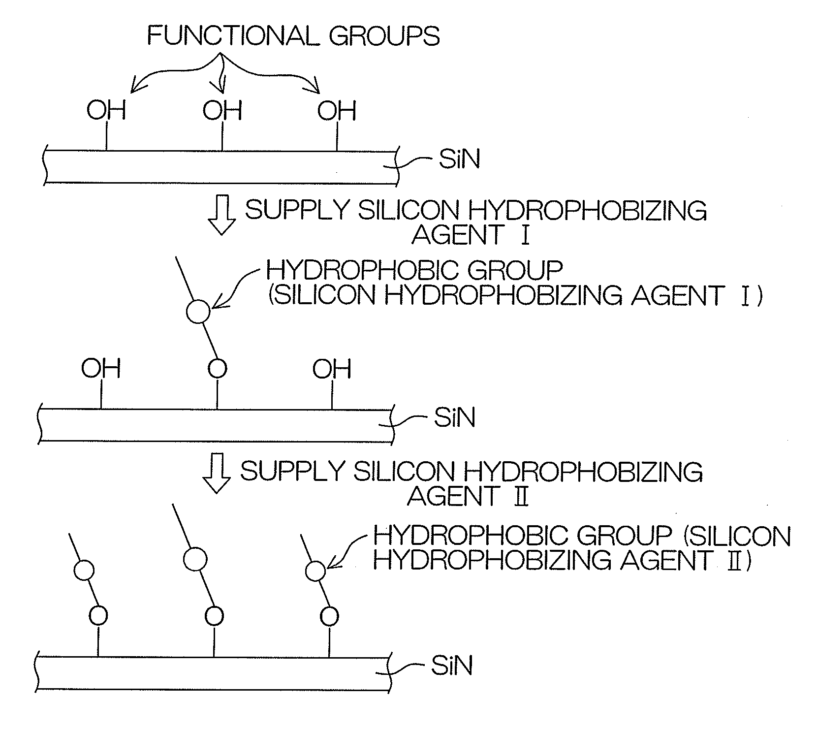
[0190]A main point of difference of the second embodiment with respect to the first embodiment is that the substrate processing apparatus 201 includes the first hydrophobizing agent supply unit 216 (hydrophobizing agent supply unit, first hydrophobizing agent supply unit) and a second hydrophobizing agent supply unit 217 (hydrophobizing agent supply unit, second hydrophobizing agent supply unit) that supply a vapor of the first hydrop...
third embodiment
[0207]FIG. 21 and FIG. 22 are schematic views of a general arrangement of a substrate processing apparatus 301 according to a third embodiment of the present invention, with each figure showing a different state.
[0208]The substrate processing apparatus 301 is a single substrate processing type substrate processing apparatus that processes a semiconductor wafer or other substrate W one at a time by a chemical solution, a rinsing liquid, and other processing liquids. The substrate processing apparatus 301 includes a spin chuck 302 (substrate holding unit) that horizontally holds and rotates the substrate W, a shielding plate 303 disposed above the spin chuck 302, and a processing liquid supply mechanism that supplies the processing liquids to the substrate W held by the spin chuck 302.
[0209]The spin chuck 302 is, for example, a gripping type chuck that grips and holds the substrate W. The spin chuck 302 includes, for example, a disk-shaped spin base 304 that is disposed horizontally, ...
PUM
| Property | Measurement | Unit |
|---|---|---|
| contact angle | aaaaa | aaaaa |
| contact angle | aaaaa | aaaaa |
| contact angle | aaaaa | aaaaa |
Abstract
Description
Claims
Application Information