Power factor correction circuit of an electronic ballast

a technology of power factor and correction circuit, which is applied in the direction of power conversion systems, instruments, light sources, etc., can solve the problem of important size of power factor correction circui

Inactive Publication Date: 2014-09-16
KONINK PHILIPS ELECTRONICS NV
View PDF10 Cites 0 Cited by
  • Summary
  • Abstract
  • Description
  • Claims
  • Application Information

AI Technical Summary

Benefits of technology

[0005]Based on understanding the prior art and issues described above, it would be advantageous to provide a power correction circuit which has a small size and which can increase the power factor of an electronic ballast. It would also be desirable to provide a power correction circuit which enables the dimmable lamp to work at a low dimming level without flickering.
[0013]It was found that a power factor correction circuit according to an embodiment of the present invention can increase the power factor of an electronic ballast to a high value such as 0.98, while the size of the power factor correction circuit is small enough to allow it to be implemented in a small size lamp. In addition, because the power factor correction circuit is coupled between the rectification circuit and the inverter, the power factor correction circuit does not directly affect the current flowing through the burner of a dimmable lamp. In this way, the dimmable lamp having the power factor correction circuit can still work well without flickering even if it is dimmed to a low dimming level.

Problems solved by technology

Firstly, the size of the power factor correction circuit is important.

Method used


Image

  • Power factor correction circuit of an electronic ballast
  • Power factor correction circuit of an electronic ballast
  • Power factor correction circuit of an electronic ballast

Examples


Embodiment Construction

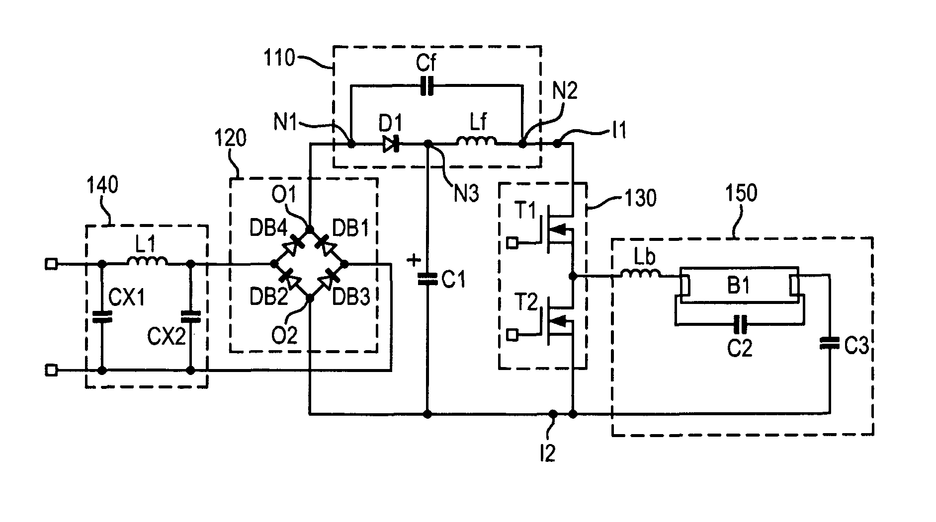
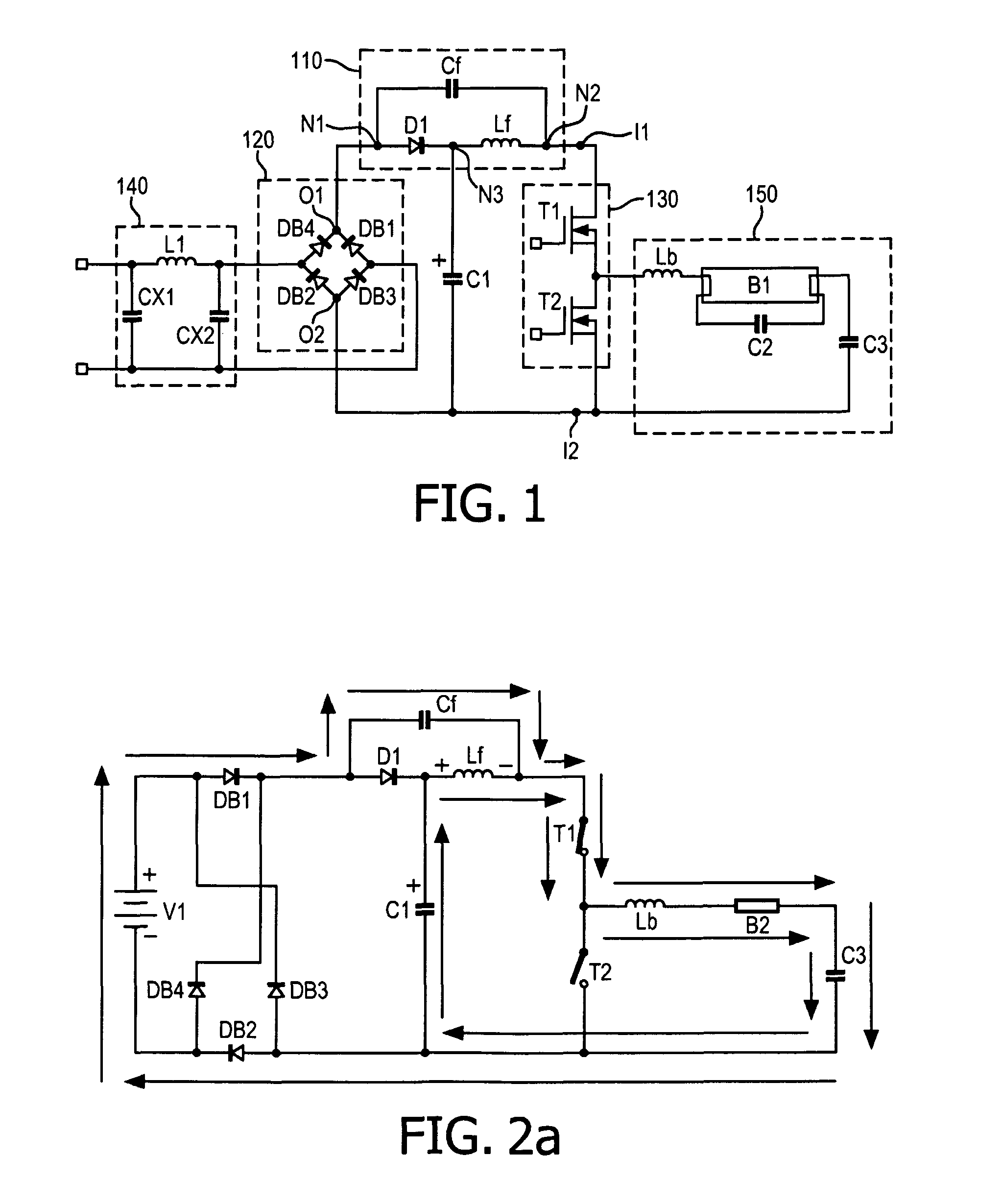
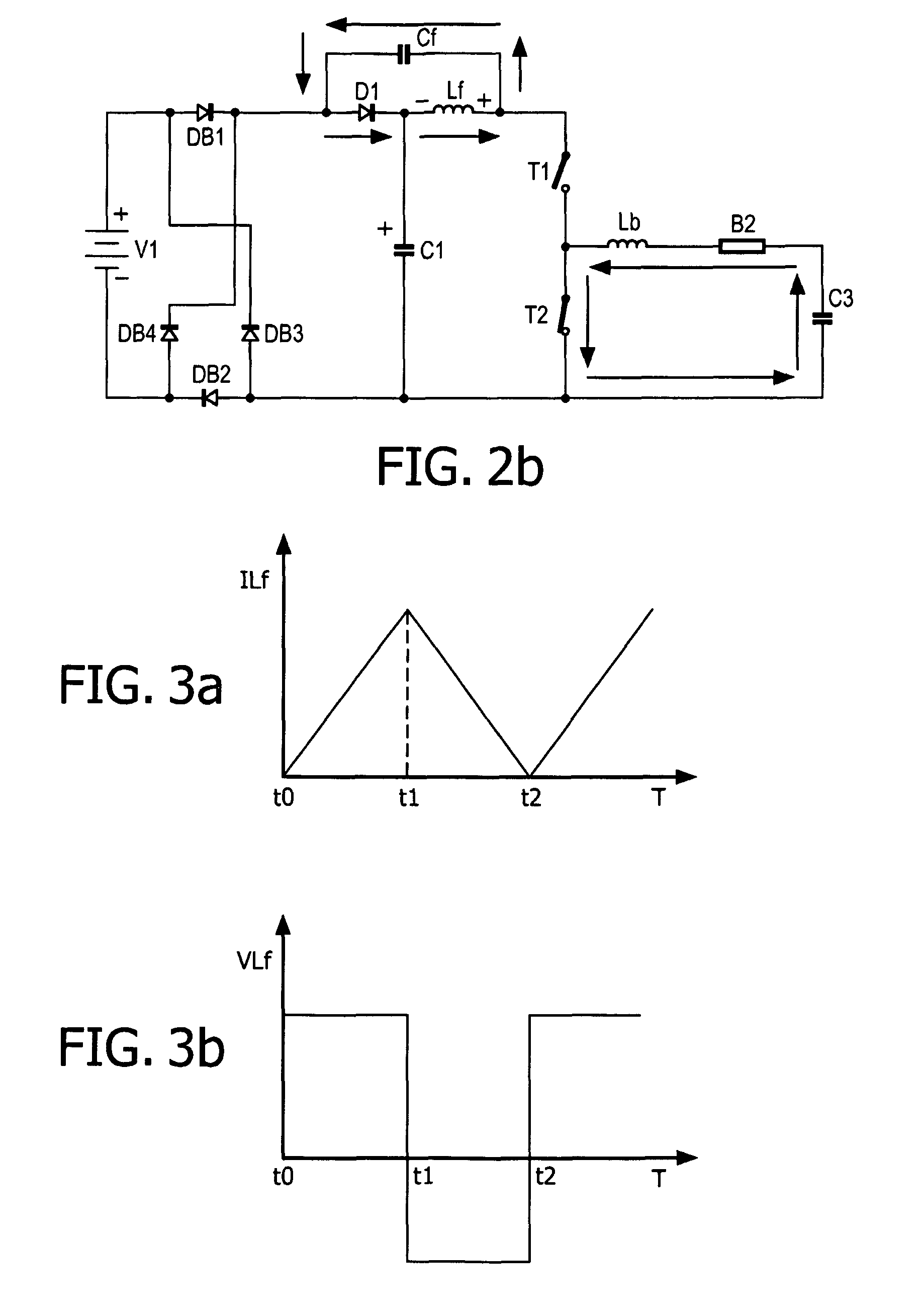
[0029]According to an embodiment of a first aspect of the invention, a power factor correction circuit of an electronic ballast is provided.

[0030]The electronic ballast includes a rectification circuit for rectifying an AC input voltage, a first capacitive element for smoothing an output voltage from the rectification circuit and an inverter.

[0031]The electronic ballast can be one of many kinds of electronic ballasts, such as a fluorescent lamp electronic ballast, an LED lamp electronic ballast, a compact fluorescent lamp electronic ballast, a cold cathode fluorescent lamp electronic ballast, a dimmable lamp electronic ballast etc. The rectification circuit can convert an AC input voltage from an AC input power source to a DC (Direct Current) voltage, and the rectification circuit can be implemented in many ways, such as a full-wave rectification circuit, a half-wave rectification circuit etc. The first capacitive element produces steady DC from a DC output of the rectification circ...


PUM


Abstract

This invention relates to a power factor correction circuit of an electronic ballast. The electronic ballast includes a rectification circuit, a first capacitive element and an inverter. The power factor correction circuit comprises a unidirectional element, an inductive element and a second capacitive element. The unidirectional element is connected in series with the inductive element, and the second capacitive element is connected in parallel with the unidirectional element and the inductive element. A junction of the unidirectional element and the second capacitive element is coupled to a first output terminal of the rectification circuit, a junction of the inductive element and the second capacitive element is coupled to an input terminal of the inverter, and the first capacitive element is coupled between a second output terminal of the rectification circuit and a junction of the unidirectional element and the inductive element.

Description

FIELD OF THE INVENTION[0001]The invention relates to a power factor correction circuit, in particular a power factor correction circuit of an electronic ballast.BACKGROUND OF THE INVENTION[0002]The power factor of an AC (alternating current) electric power system is defined as the ratio of the real power to the apparent power, and is a number between 0 and 1. In an electric power system, a load with a low power factor draws more current than a load with a high power factor for the same amount of useful power transferred, and the higher currents increase the energy lost in the distribution system.[0003]Linear loads with a low power factor can be corrected with a passive power factor correction circuit. Non-linear loads, such as rectifiers, distort the current drawn from the electric power system. In such cases, an active or passive power factor correction circuit may be used to counteract the distortion and raise the power factor.SUMMARY OF THE INVENTION[0004]The inventor of the pres...

Claims


Application Information

Patent Timeline
Patent Type & Authority Patents(United States)
IPC IPC(8): H05B41/24H02M1/42H05B37/00H05B41/28
CPCH05B37/00H02M1/42H05B41/28H05B47/10
Inventor WU, JUN
Owner KONINK PHILIPS ELECTRONICS NV
Why Eureka
Try Eureka