Method of manufacturing multi-layer circuit board, and multi-layer circuit board

a manufacturing method and technology of multi-layer circuit boards, applied in the direction of printed circuit manufacturing, printed circuit assembling, printed circuit aspects, etc., can solve the problems of difficult to form a minute outer layer circuit, risk of cost rise, yield drop, etc., to ensure the flatness of an outer layer substrate, improve yield, and low cost

Active Publication Date: 2014-11-11
FUJIKURA PRINTED CIRCUITS LTD
View PDF2 Cites 6 Cited by
  • Summary
  • Abstract
  • Description
  • Claims
  • Application Information

AI Technical Summary

Benefits of technology

[0017]The present invention allows yield to be improved while ensuring flatness of an outer layer substrate, easily and at low cost.

Problems solved by technology

However, in the conventional method of manufacturing disclosed in the above-mentioned Document 1, alignment of each of materials during actual manufacturing is difficult, hence whether intrusion of chemicals into the terminal portion can be reliably prevented or not is highly reliant on accuracy of alignment, resulting in a risk that costs rise and also yield falls.
Moreover, there is a problem that because stacking is performed after forming the opening in the interlayer adhesive layer, an overall substrate thickness of the opening portion is small compared to that of other portions, hence pressure is insufficient during stacking thereby generating irregularity in the outer layer substrate and thus making it difficult to form a minute outer layer circuit.

Method used


Image

  • Method of manufacturing multi-layer circuit board, and multi-layer circuit board
  • Method of manufacturing multi-layer circuit board, and multi-layer circuit board
  • Method of manufacturing multi-layer circuit board, and multi-layer circuit board

Examples


first embodiment

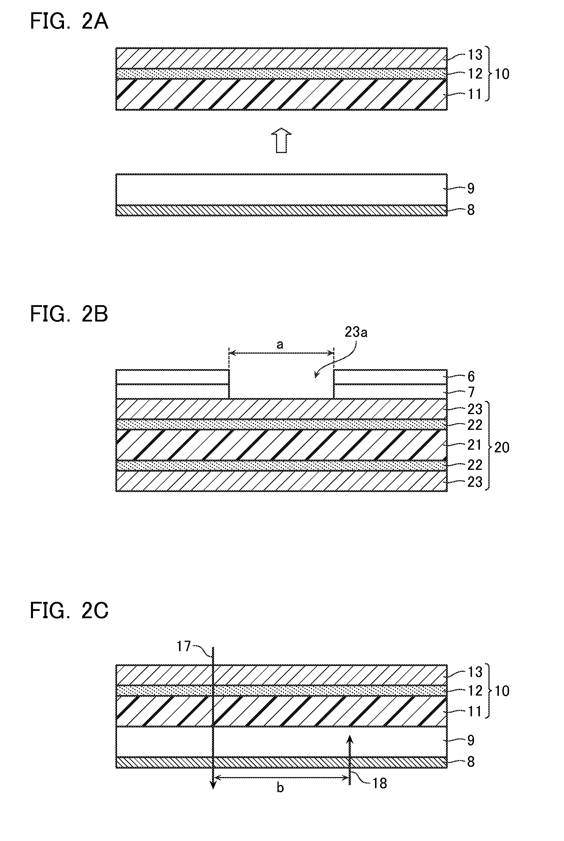
[0040]FIG. 1 is a flowchart showing manufacturing processes of a multi-layer circuit board according to a first embodiment of the present invention. FIGS. 2A, 2B, 2C, 2D, 2E and 2F are cross-sectional diagrams showing this multi-layer circuit board in sequence of manufacturing processes. FIGS. 3A, 3B and 3C are cross-sectional diagrams showing in enlargement a concept of part of manufacturing processes of this multi-layer circuit board. FIGS. 4A, 4B, 4C and 4D are perspective diagrams showing a part of manufacturing processes of this multi-layer circuit board. FIG. 5 is a cross-sectional view showing a completed article of the multi-layer circuit board. First, as shown in FIG. 2A, an outer layer substrate 10 comprising a single-sided copper-clad laminate (single-sided CCL) having a conductor layer 13 of copper foil or the like applied to a base substrate 11 via an adhesive agent 12, is prepared.

[0041]The base substrate 11 is configured by a resin film, for example. The following may...

second embodiment

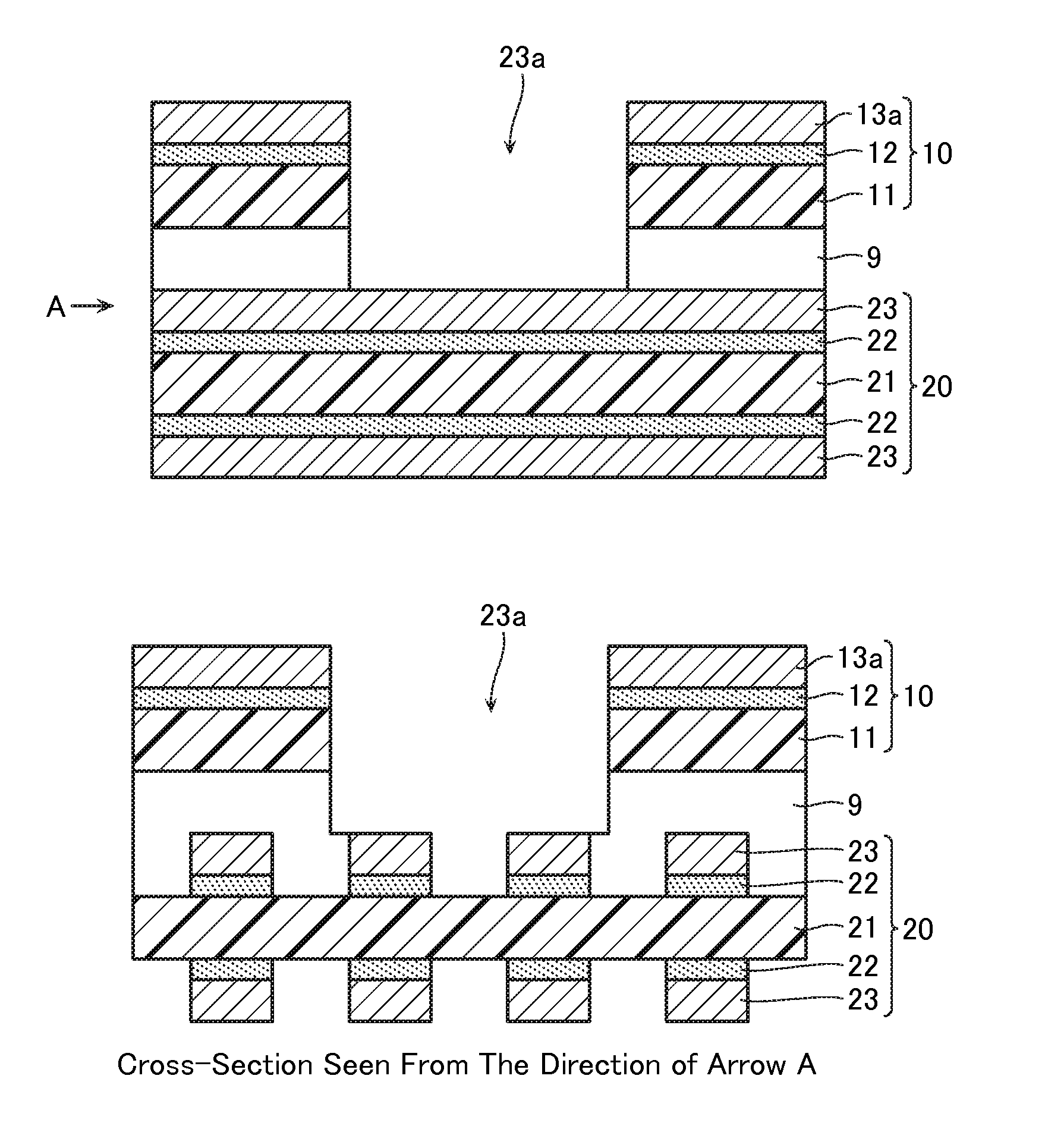
[0057]FIG. 6 is a cross-sectional diagram showing a multi-layer circuit board according to a second embodiment of the present invention. FIG. 7 is a cross-sectional diagram of FIG. 6 as seen from the direction of arrow A. FIGS. 8A and 8B are cross-sectional diagrams showing the multi-layer circuit board in sequence of manufacturing processes. As shown in FIGS. 6 and 7, the multi-layer circuit board according to the second embodiment differs from the multi-layer circuit board according to the first embodiment in not having an adhesive agent 7 and a cover lay 6 provided on the inner layer circuit 23 of the inner layer substrate 20.

[0058]That is, as shown in FIGS. 6 and 7, in the multi-layer circuit board, the outer layer substrate 10 and the inner layer substrate 20 are stacked upon direct adhesion of the inner layer circuit 23 of the inner layer substrate 20 and the adhesive layer 9. The region where the residual exfoliating paper 8a (not illustrated) has been disposed beforehand on ...

third embodiment

[0063]A method of manufacturing a multi-layer circuit board according to a third embodiment differs from the methods of manufacturing a multi-layer circuit board according to the first and second embodiments as follows. That is, in the method of manufacturing a multi-layer circuit board according to the third embodiment, as shown in FIG. 9, the exfoliating paper 8 provided in the outer layer substrate 10 is cut so as to cover the region corresponding to the circuit exposure portion 23a of the inner layer circuit 23 and attached to the adhesive layer 9, in advance. This differs from the methods of manufacturing a multi-layer circuit board according to the first and second embodiments. Note that masking tape or the like may be employed in place of the exfoliating paper 8 as a mask material. According to the embodiment, as shown in FIG. 10, step for applying a mask material having a size covering the circuit exposure portion 23a to the adhesive layer 9 of the outer layer substrate 10 s...


PUM

PropertyMeasurementUnit
temperatureaaaaaaaaaa
areaaaaaaaaaaa
sizeaaaaaaaaaa

Abstract

A multi-layer circuit board having a connector portion of an inner layer substrate being exposed, the multi-layer circuit board comprising: an inner layer substrate in which an inner layer circuit is formed, the inner layer circuit including the connector portion; and an outer layer substrate having an outer layer circuit formed on an insulating layer and having a region corresponding to the connector portion peeled off, an inner layer circuit side of the inner layer substrate and an insulating layer side of the outer layer substrate being adhered to one another via an adhesive layer so as to face one another, and a conductor layer other than the connector portion of the inner layer circuit being adhered to the outer layer substrate directly by the adhesive layer.

Description

CROSS-REFERENCE TO RELATED APPLICATIONS[0001]This application is based upon and claims the benefit of priority from the prior Japanese Patent Application No. 2011-232220, filed on Oct. 21, 2011, the entire contents of which are incorporated herein by reference.BACKGROUND OF THE INVENTION[0002]1. Field of the Invention[0003]The present invention relates to a method of manufacturing a multi-layer circuit board, and to the multi-layer circuit board.[0004]2. Description of the Related Art[0005]Regarding multi-layer circuit boards in which an inner layer substrate including an inner layer circuit and an outer layer substrate including an outer layer circuit are stacked, a method of manufacturing such a multi-layer circuit board that has a structure exposing a part of the inner layer circuit disclosed in Unexamined Japanese Patent Application Publication No. 2010-206124 A is known (refer to, Document 1). This multi-layer circuit board is manufactured as follows. That is, the outer layer s...

Claims


Application Information

Patent Timeline
Patent Type & Authority Patents(United States)
IPC IPC(8): H05K1/03H05K3/46
CPCH05K3/4611H05K2203/0264H05K3/4697H05K2201/09127H05K2201/0909H05K2203/1572H05K2203/0228Y10T29/49124Y10T29/49144
Inventor INATANI, YUJI
Owner FUJIKURA PRINTED CIRCUITS LTD
Why Eureka
Try Eureka