Memory device and read operation method thereof

a memory device and read operation technology, applied in the field of memory devices and read operation methods, can solve the problems of reducing the read margin of sensing erase cells, circuit area and current consumption become important issues, etc., and achieve the effect of reducing the setup time of signal lines in page read

Active Publication Date: 2014-11-18
MACRONIX INT CO LTD
View PDF3 Cites 2 Cited by
  • Summary
  • Abstract
  • Description
  • Claims
  • Application Information

AI Technical Summary

Benefits of technology

[0005]Embodiments of a memory device and a reading operation method thereof are disclosed. During sensing, the charged global bit lines (which are heavy loading) and the charged word lines (which are heavy loading too) are kept charged, for reducing signal line setup (charge) time in page read.

Problems solved by technology

Thus, the circuit area and the current consumption become important issues.
Further, during parallel sensing for multiple bits, the common source level may be raised due to large read current flowing through drain sides and accordingly the read margin for sensing erase cells is reduced and thus undesired.

Method used


Image

  • Memory device and read operation method thereof
  • Memory device and read operation method thereof
  • Memory device and read operation method thereof

Examples


first embodiment

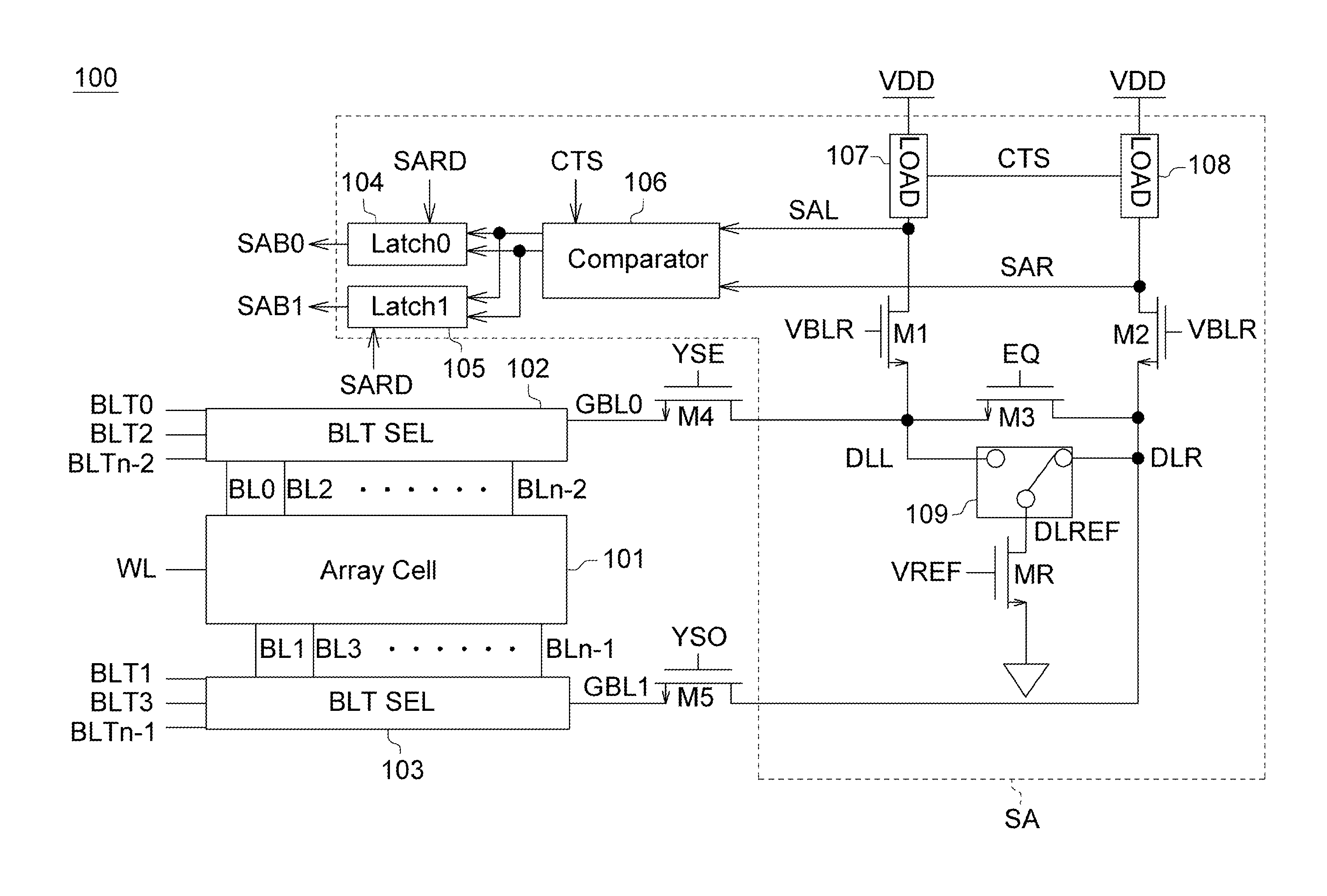
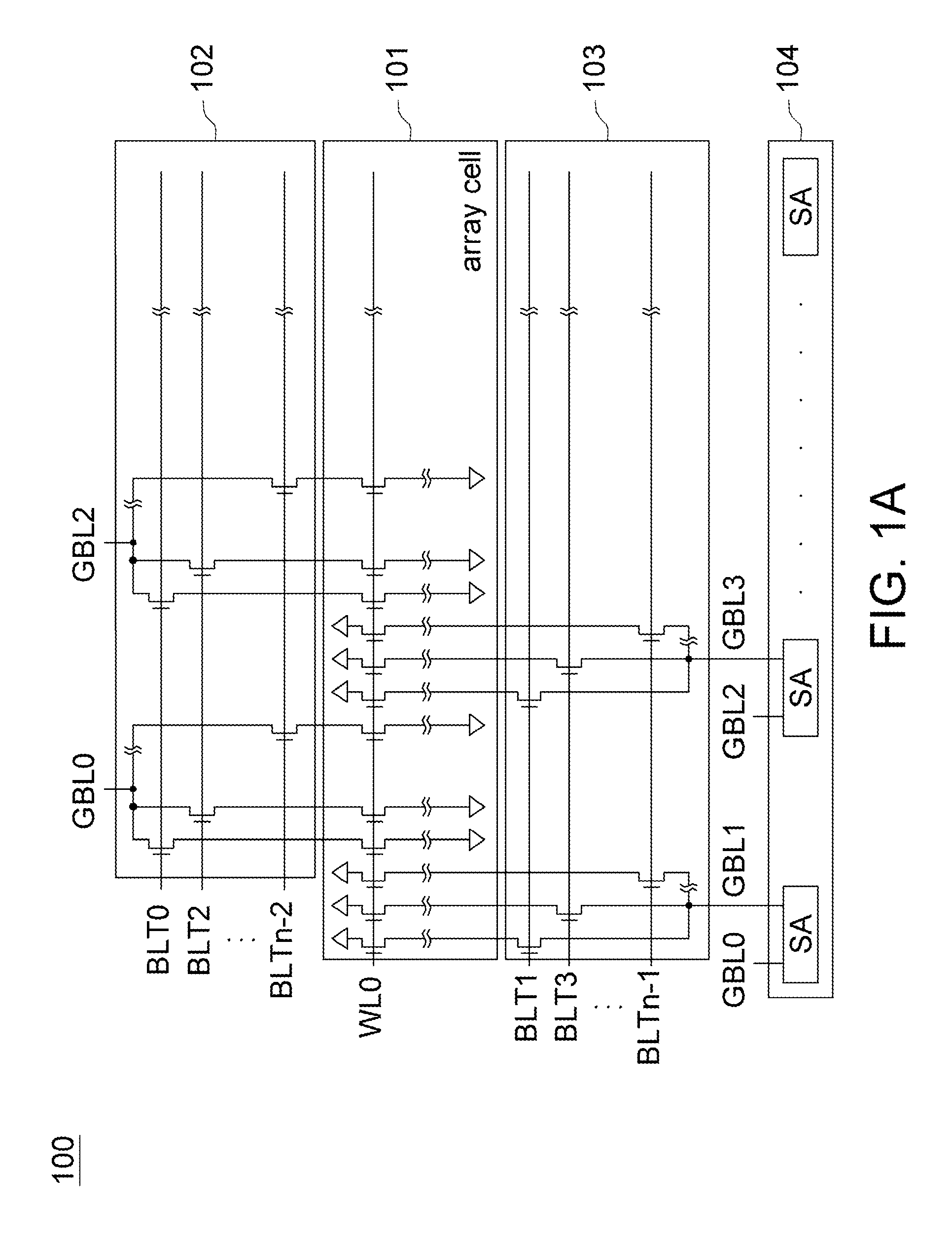
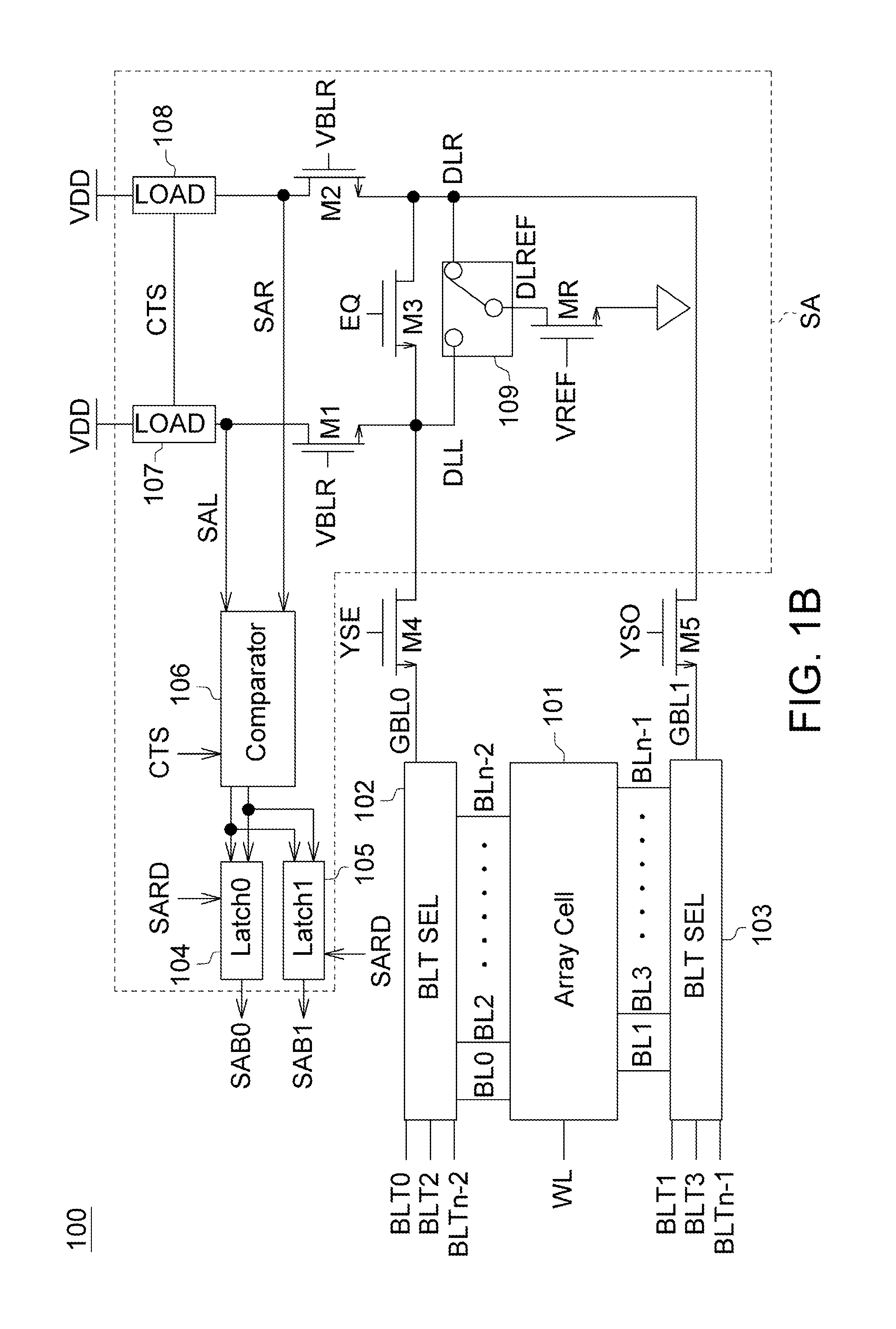
[0016]FIG. 1A shows a simplified diagram and FIG. 1B shows a function block diagram of a memory device according to a first embodiment of the disclosure. As shown in FIG. 1A, the memory device 100 according to the first embodiment of the disclosure at least includes an array cell 101, bit line selectors 102˜103 and a sensing amplifier circuit 104. The array cell 101 has a plurality of memory cells arranged in an array. The bit line selector 102 includes a plurality of bit line selection transistors for selectively conducting the global bit lines GBL0, GBL2 . . . to the array cell 101 according to the bit line selection signals BLT0, BLT2 . . . BLTn-2. Similarly, the bit line selector 103 includes a plurality of bit line selection transistors for selectively conducting the global bit lines GBL1, GBL 3 . . . to the array cell 101 according to the bit line selection signals BLT1, BLT3 . . . BLTn-1. The sensing amplifier circuit 104 has a plurality of sensing amplifiers SA. Each SA in t...

second embodiment

[0034]FIG. 5 shows a function block diagram of a memory device according to a second embodiment of the disclosure. As shown in FIG. 5, the memory device 500 according to the second embodiment of the disclosure at least includes an array cell 501, bit line selectors 502˜503 and a sensing amplifier circuit (not shown). The SA includes latches 504˜505, a comparator 506, loads 507A˜508B, a reference side selector 509, multiplexers 510˜513 and transistors MR, M1A˜M3B. The array cell 501, the bit line selectors 502˜503, the latches 504˜505, the comparator 506, the loads 507A˜508B, the reference side selector 509 and the transistors MR, M1A˜M5B are the same or similar to that in the first embodiment and thus their details are omitted. The control signal A3 controls the MUXs 510˜513 for the first half page reading and for the second half page reading.

[0035]The timing waveform of the second embodiment 500 of the disclosure is shown in FIG. 6.

[0036]At the WL / GBL / BL setup phase, the control si...

third embodiment

[0042]FIG. 7 shows a function block diagram of a memory device according to a third embodiment of the disclosure. As shown in FIG. 7, the memory device 700 according to the third embodiment of the disclosure at least includes an array cell 701, bit line selectors 702˜703 and a sensing amplifier circuit (not shown). The SA includes latches 704˜705, a comparator 706, loads 707A˜708, a reference side selector 709, multiplexers 710˜712 and transistors MR, M1A˜M3B. The SA in the third embodiment has similar structure and operation to that in the second embodiment and thus the details are omitted. The control signal A6 controls the reference side selector 709 and the multiplexers 711˜712. During read operation, the signals YES0 and YEO0 are both high. If the control signal is L, the node DLL0 is connected to the global bit line GBL0 via the MUX 712; the node DLL1 is connected to the global bit line GBL2 via the MUX 711; and the node DLREF is connected to the global bit line GBL1 via the r...


PUM


Abstract

A read operation for a memory device. In response to an input address indicating to read data from a different page, a selected word line, first and second global bit lines and a selected first bit line group are precharged. A first cell current flowing through the selected word line, the first and the selected first bit line groups is generated. A first reference current flowing through the second global bit line group is generated. A first half page data is read based on the first cell current and the first reference current. The selected word line, the first and the second global bit lines are kept precharged. A second cell current flowing through the selected word line is generated. A second reference current is generated. A second half page data is read based on the second cell current and the second reference current.

Description

TECHNICAL FIELD[0001]The present disclosure relates in general to a memory device and a read operation method thereof.BACKGROUND[0002]In recent years, non-volatile memories that are data-rewritable semiconductor devices are widely used.[0003]In memory reading, an output current is obtained by applying a word line reference voltage to a gate of the memory cell and applying a bit line voltage to source / drain of the memory cell. Then, the output current is compared with a reference current to determine the bit stored in the memory cell.[0004]In memory, sense amplifiers are used for bit reading. For example, for a memory cell of 256 M, it may require 1K (i.e. 1024) sensing amplifiers for data sensing / reading. For reading a page data for example including 256 bits, 256 sensing amplifiers in a SA circuit (for example having 1K sensing amplifiers) concurrently operate for sensing 256 bits. If the memory cell is larger, more sensing amplifiers may be needed. Thus, the circuit area and the c...

Claims


Application Information

Patent Timeline
Patent Type & Authority Patents(United States)
IPC IPC(8): G11C7/10G11C7/08G11C16/28G11C7/18G11C7/12
CPCG11C7/1048G11C7/12G11C2207/002G11C7/08G11C7/18G11C7/106G11C7/06
Inventor CHANG, CHIN-HUNGCHEN, CHIA-JUNGLO, SU-CHUEHCHEN, KEN-HUICHANG, KUEN-LONG
Owner MACRONIX INT CO LTD
Why Eureka
Try Eureka