Method for manufacturing light-emitting device

a technology of light-emitting devices and manufacturing methods, which is applied in the direction of organic semiconductor devices, sustainable manufacturing/processing, and final product manufacturing, etc., can solve the problems of reducing the reliability of light-emitting devices, easy deterioration of metal elements, etc., and achieve the effect of preventing the occurrence of shape defects and reducing the cost of production

Active Publication Date: 2014-12-16
SEMICON ENERGY LAB CO LTD
View PDF15 Cites 30 Cited by
  • Summary
  • Abstract
  • Description
  • Claims
  • Application Information

AI Technical Summary

Benefits of technology

[0008]However, the EL element easily deteriorates due to a contaminant such as moisture which enters from outside and this deterioration is one of the factors that reduce reliability of a light-emitting device.
[0009]Thus, an object of one embodiment of the present invention is to provide a more convenient highly reliable light-emitting device which can be used for a variety of applications. Another object of one embodiment of the present invention is to manufacture, without complicating the process, a highly reliable light-emitting device having a shape suitable for its intended purpose.
[0010]In a manufacturing process of a light-emitting device, a light-emitting panel is manufactured which is at least partly curved by processing the shape to be molded after the manufacture of an electrode layer and / or an element layer, and a protective film covering a surface of the light-emitting panel which is at least partly curved is formed, so that a light-emitting device using the light-emitting panel has a more useful function and higher reliability.

Problems solved by technology

However, the EL element easily deteriorates due to a contaminant such as moisture which enters from outside and this deterioration is one of the factors that reduce reliability of a light-emitting device.

Method used


Image

  • Method for manufacturing light-emitting device
  • Method for manufacturing light-emitting device
  • Method for manufacturing light-emitting device

Examples


embodiment 1

[Embodiment 1]

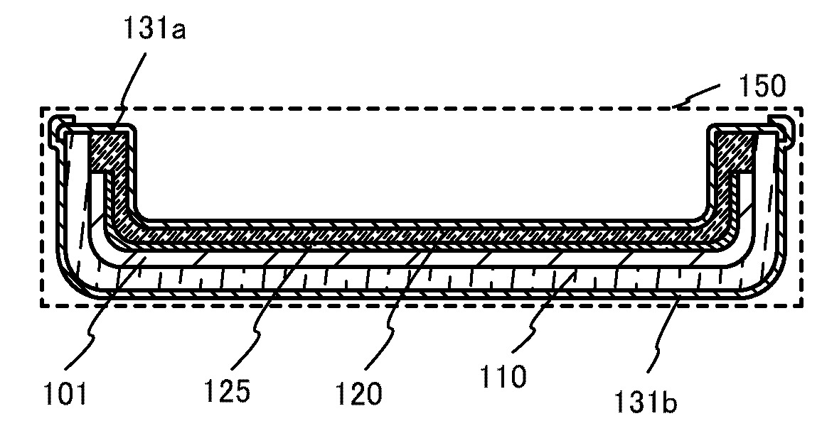
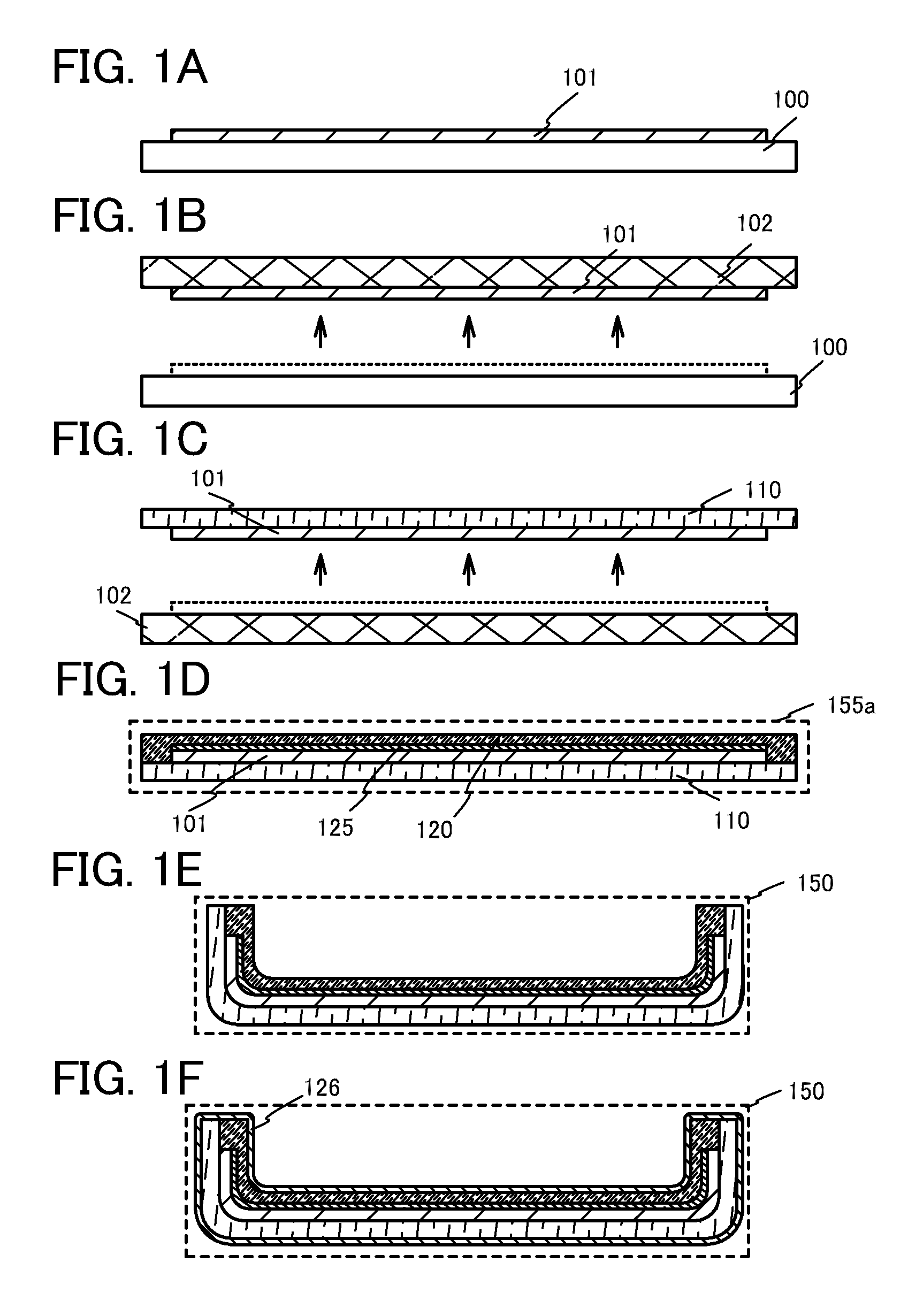
[0039]A light-emitting device will be described with reference to FIGS. 1A to 1F and FIGS. 5A and 5B.

[0040]FIGS. 1A to 1F and FIGS. 5A and 5B are cross-sectional views illustrating a light-emitting device and a method for manufacturing a light-emitting device.

[0041]The light-emitting device includes a light-emitting element having at least a first electrode layer, an EL layer, and a second electrode layer; and a pair of sealing members which seals the light-emitting element therebetween. The light-emitting device may also be provided with a semiconductor element, preferably a thin film transistor. In the case of an active matrix light-emitting device, a driving thin film transistor is provided in each pixel.

[0042]Although an active matrix light-emitting device is shown as an example in this embodiment, this embodiment can also be applied to a passive matrix light-emitting device.

[0043]In this embodiment, a light-emitting panel is manufactured which is at least partly c...

embodiment 2

[Embodiment 2]

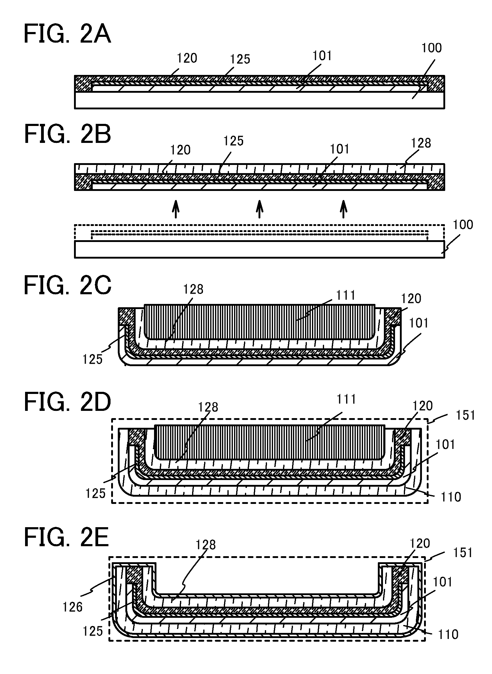
[0079]In this embodiment, another example of a method for manufacturing a light-emitting device, which is different from that shown in Embodiment 1, will be described with reference to FIGS. 2A to 2E. Therefore, the light-emitting device of this embodiment, except a different part, can be manufactured in a manner similar to that shown in Embodiment 1; thus, description of the same components or components having the same functions as Embodiment 1, and the manufacturing process thereof will be omitted.

[0080]FIGS. 2A to 2E are cross-sectional views illustrating a light-emitting device and a method for manufacturing the light-emitting device.

[0081]In this embodiment, a light-emitting panel is manufactured which is at least partly curved by processing the shape to be molded after the manufacture of an electrode layer and / or an element layer, and a protective film covering a surface of the light-emitting panel which is at least partly curved is formed, so that a light-emitt...

embodiment 3

[Embodiment 3]

[0097]In this embodiment, an example of a light-emitting device in Embodiment 1 or Embodiment 2, which uses a supporting member, will be described with reference to FIGS. 3A to 3C and FIGS. 4A to 4C. Therefore, the light-emitting device of this embodiment, except a different part, can be manufactured in a manner similar to that shown in Embodiment 1 or Embodiment 2; thus, description of the same components or components having the same functions as Embodiment 1 or Embodiment 2, and the manufacturing process thereof will be omitted.

[0098]FIGS. 3A to 3C and FIGS. 4A to 4C illustrate the light-emitting device of this embodiment.

[0099]In a manufacturing process of a light-emitting device in this embodiment, the shape of a light-emitting panel is processed to be molded after the manufacture of an electrode layer and / or an element layer, so that a light-emitting device using the light-emitting panel has a more useful function. Furthermore, the provision of a protective film ...


PUM

PropertyMeasurementUnit
wavenumberaaaaaaaaaa
frequencyaaaaaaaaaa
temperatureaaaaaaaaaa

Abstract

An object of one embodiment of the present invention is to provide a more convenient highly reliable light-emitting device which can be used for a variety of applications. Another object of one embodiment of the present invention is to manufacture, without complicating the process, a highly reliable light-emitting device having a shape suitable for its intended purpose. In a manufacturing process of a light-emitting device, a light-emitting panel is manufactured which is at least partly curved by processing the shape to be molded after the manufacture of an electrode layer and / or an element layer, and a protective film covering a surface of the light-emitting panel which is at least partly curved is formed, so that a light-emitting device using the light-emitting panel has a more useful function and higher reliability.

Description

BACKGROUND OF THE INVENTION[0001]1. Field of the Invention[0002]The present invention relates to a light-emitting device and a manufacturing method thereof.[0003]2. Description of the Related Art[0004]In recent years, light-emitting devices have been used in a variety of places for a variety of applications and therefore have been required to have various characteristics and shapes. Accordingly, light-emitting devices serving their intended purposes have been actively developed.[0005]For example, as a light-emitting device which is provided for an amusement machine, a display whose display surface is curved so that players can experience stereoscopic effect has been reported (e.g., see Patent Document 1).[0006]As the light-emitting device, a light-emitting device having a light-emitting element (hereinafter also referred to as an EL element) exhibiting electroluminescence (hereinafter also referred to as EL), which is lightweight and can realize high contrast and wide viewing angle,...

Claims


Application Information

Patent Timeline
Patent Type & Authority Patents(United States)
IPC IPC(8): H01L21/30H01L51/52H01L51/00H01L51/56
CPCH01L51/56Y02E10/549H01L51/5237H01L51/0097H01L2251/5338Y10T29/49117H01L51/5253H01L27/3244Y02P70/50H10K59/12H10K77/111H10K50/8426H10K50/844H10K71/851H10K2102/311H10K71/00H10K50/84
Inventor YAMAZAKI, SHUNPEIHATANO, KAORU
Owner SEMICON ENERGY LAB CO LTD
Why Eureka
Try Eureka