Method for fabricating integrated circuit with different gate heights and different materials

a technology of integrated circuits and gate heights, applied in the direction of semiconductor/solid-state device manufacturing, basic electric elements, electric apparatus, etc., can solve the problems of leakage current and thin gate insulation layer of silicon oxide, and achieve the effect of reducing process costs and consuming time, and simplifying process

Active Publication Date: 2014-12-30
UNITED MICROELECTRONICS CORP
View PDF9 Cites 0 Cited by
  • Summary
  • Abstract
  • Description
  • Claims
  • Application Information

AI Technical Summary

Benefits of technology

The present invention provides a method for integrating high-k / metal gate semiconductor devices with poly-silicon semiconductor devices having different heights. This method simplifies the fabrication process and reduces costs and time consumption.

Problems solved by technology

However, a leakage current occurs when the gate insulation layer of silicon oxide becomes thinner.

Method used


Image

  • Method for fabricating integrated circuit with different gate heights and different materials
  • Method for fabricating integrated circuit with different gate heights and different materials
  • Method for fabricating integrated circuit with different gate heights and different materials

Examples


first embodiment

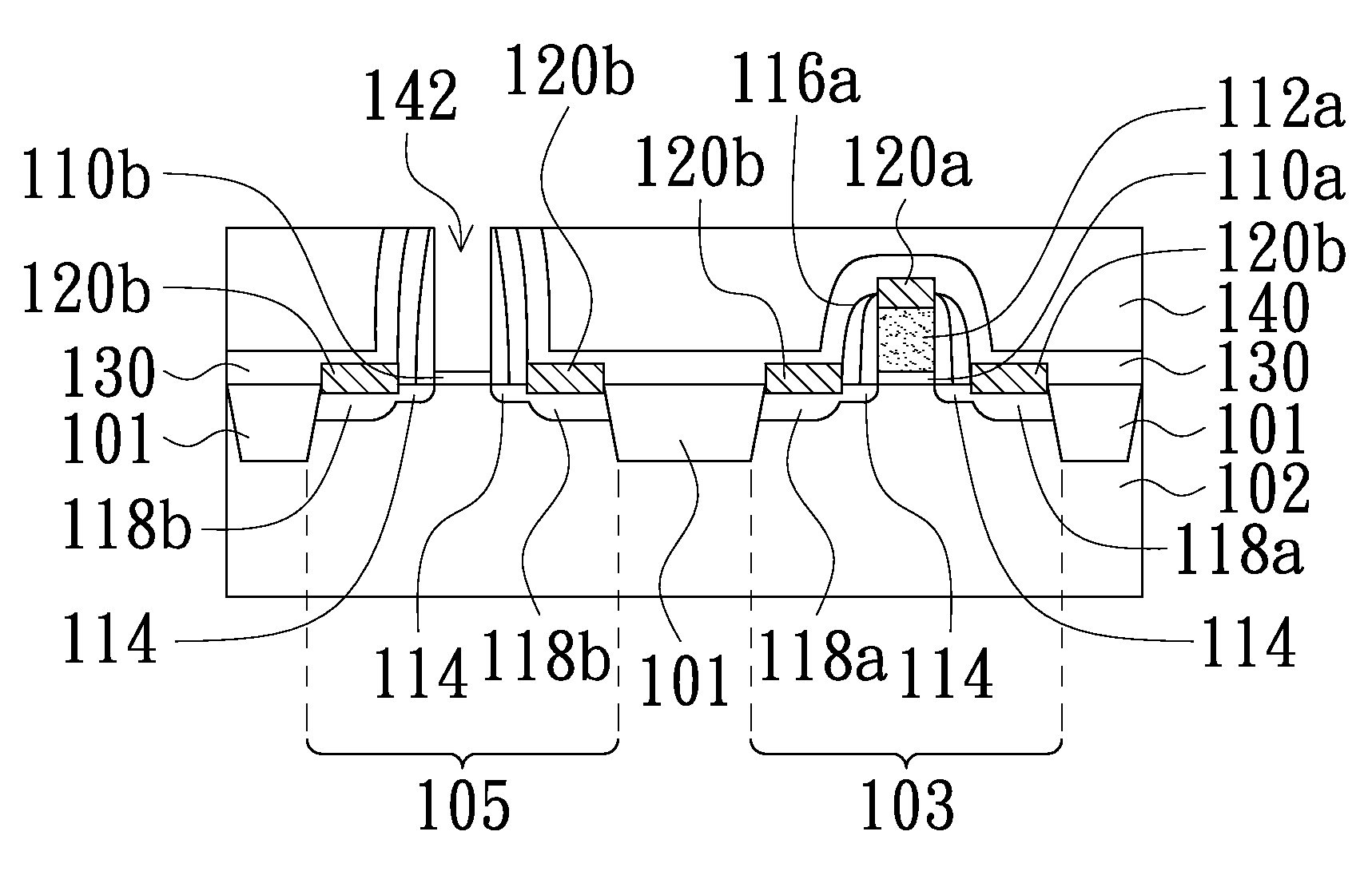
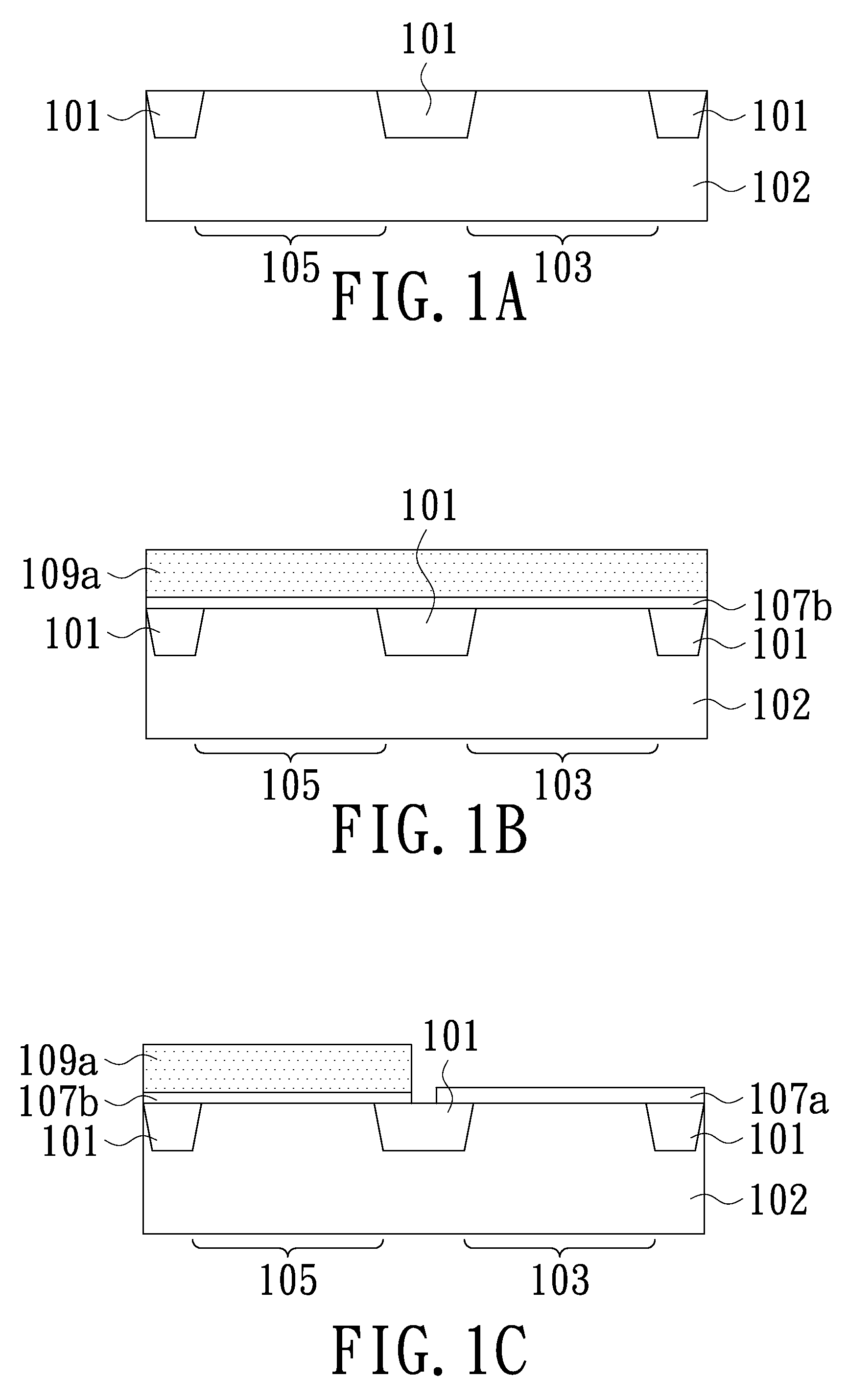
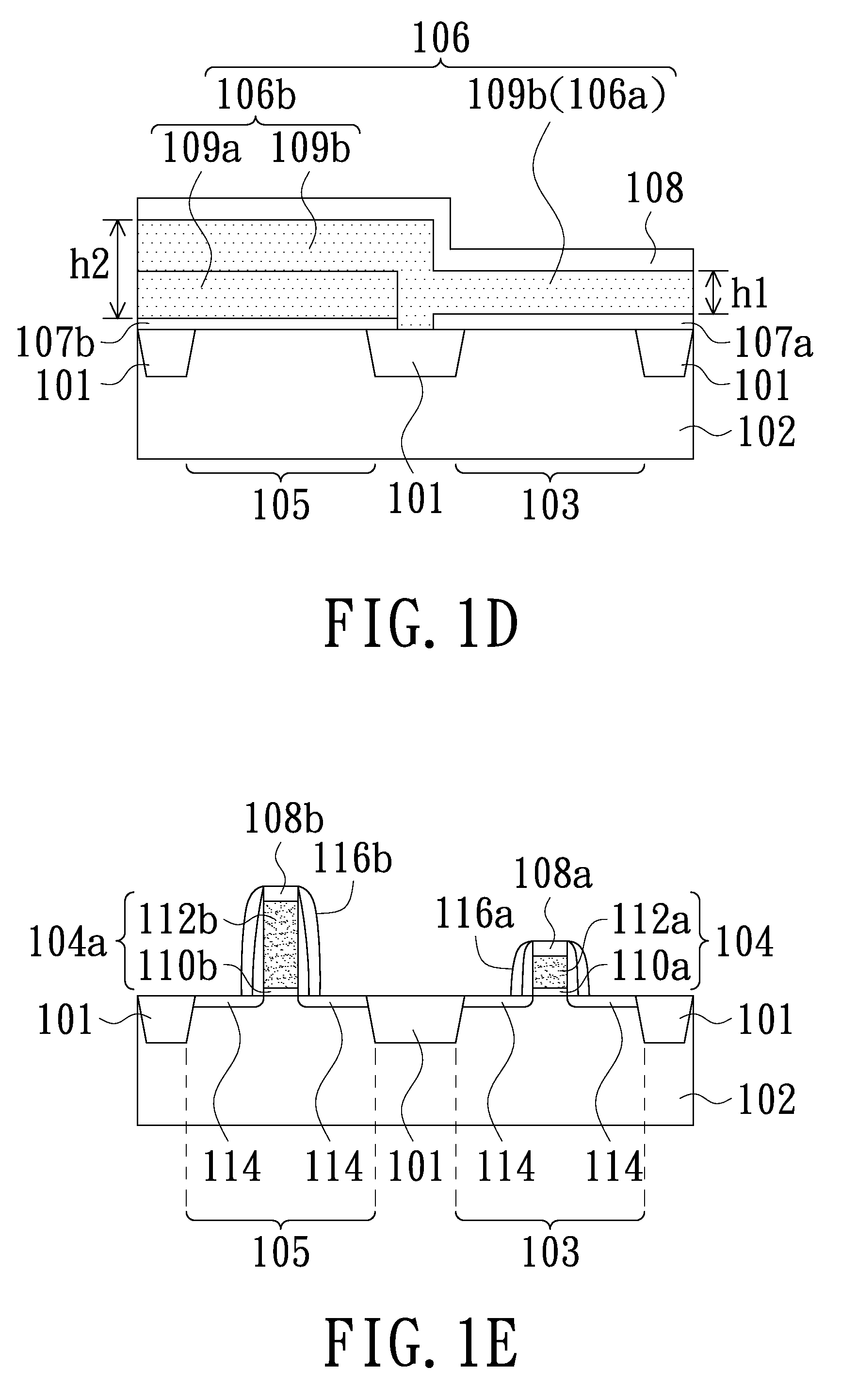
[0026]FIGS. 1A-1K illustrate cross-section views of an integrated circuit during a fabricating process thereof according to the present invention. Referring to FIGS. 1A-1E, a substrate 102, such as a silicon substrate, a silicon-containing substrate, or a silicon-on-insulator (SOI) substrate, with a plurality of isolation structures 101 formed therein is provided. Moreover, a first active region 103 and a second active region of the substrate 102 are defined by the isolation structures 101. Accordingly, one of the isolation structures 101 is located between the first active region 103 and the second active region 105. In this embodiment, the isolation structures 101 are, for example, shallow trench isolation (STI) structures or filed oxide isolation structures.

[0027]As shown in FIG. 1E, a first stacked structure 104 has been foamed on the first active region 103 of the substrate 102 and a second stacked structure 104a has been formed on the second active region 105. The first stacke...

second embodiment

[0052]FIGS. 2A-2E illustrate cross-section views of an integrated circuit during the fabricating process thereof according to the present invention. Referring to FIG. 2A, in this embodiment, the method of forming the gate material layer includes, for example, forming a first dielectric material layer 107a and a poly-silicon layer 206 sequentially on the substrate 102 to cover the first active region 103 and the second active region 105. The poly-silicon layer 206 has the second thickness h2. The first dielectric material layer 107a may be, for example, at least one of oxide layer and nitride layer.

[0053]Referring to FIG. 2B, a portion of the poly-silicon layer 206 is removed for thinning the portion of the poly-silicon layer 206 located above the first active region 103 to the first thickness h1. Therefore, the gate material layer 106 having a first portion 106a and the second portion 106b is formed. Then, a mask layer 108 is optional formed on the gate material layer 106.

[0054]Afte...


PUM


Abstract

A method for fabricating an integrated circuit includes the following steps of: providing a substrate with at least one isolation structure formed therein so as to separate the substrate into a first active region with a first stacked structure formed thereon and a second active region with a second stacked structure formed thereon; forming an interlayer dielectric layer covering the first stacked structure and the second stacked structure; and planarizing the interlayer dielectric layer to expose the top surface of the first stacked structure, wherein the second stacked structure is still covered by the interlayer dielectric layer after planarizing.

Description

CROSS-REFERENCE TO RELATED APPLICATIONS[0001]This application is a divisional of, and claims the benefit of U.S. nonprovisional application Ser. No. 13 / 412714, filed Mar. 6, 2012, the disclosure of which is hereby incorporated by reference herein in its entirety.TECHNICAL FIELD[0002]The present invention relates to a method for fabricating an integrated circuit, more particularly to a method for fabricating an integrated circuit integrating the high-k / metal gate semiconductor device with the poly-silicon semiconductor device.DESCRIPTION OF THE RELATED ART[0003]As the dimension of a semiconductor device is getting less, the dimension of the gate structure and the thickness of the gate insulation layer are reduced accordingly. However, a leakage current occurs when the gate insulation layer of silicon oxide becomes thinner. To reduce the leakage current, a high dielectric constant (high-k) material is used to replace silicon oxide for forming the gate insulation layer. The gate of pol...

Claims


Application Information

Patent Timeline
Patent Type & Authority Patents(United States)
IPC IPC(8): H01L21/8238H01L21/8234
CPCH01L21/823807H01L21/823842H01L21/823835H01L21/82345H01L21/823857
Inventor LEE, HSIANG-CHENSHIH, PING-CHIACHEN, KE-CHIWANG, CHIH-MINGHUANG, CHI-CHENG
Owner UNITED MICROELECTRONICS CORP
Why Eureka
Try Eureka