Liquid crystal display device and manufacturing method for same
a technology of liquid crystal display and manufacturing method, which is applied in semiconductor devices, instruments, chemistry apparatus and processes, etc., can solve the problems of small aperture ratio of pixels, abnormal alignment of proportions, and narrow surrounded signal lines
- Summary
- Abstract
- Description
- Claims
- Application Information
AI Technical Summary
Benefits of technology
Problems solved by technology
Method used
Image
Examples
first embodiment
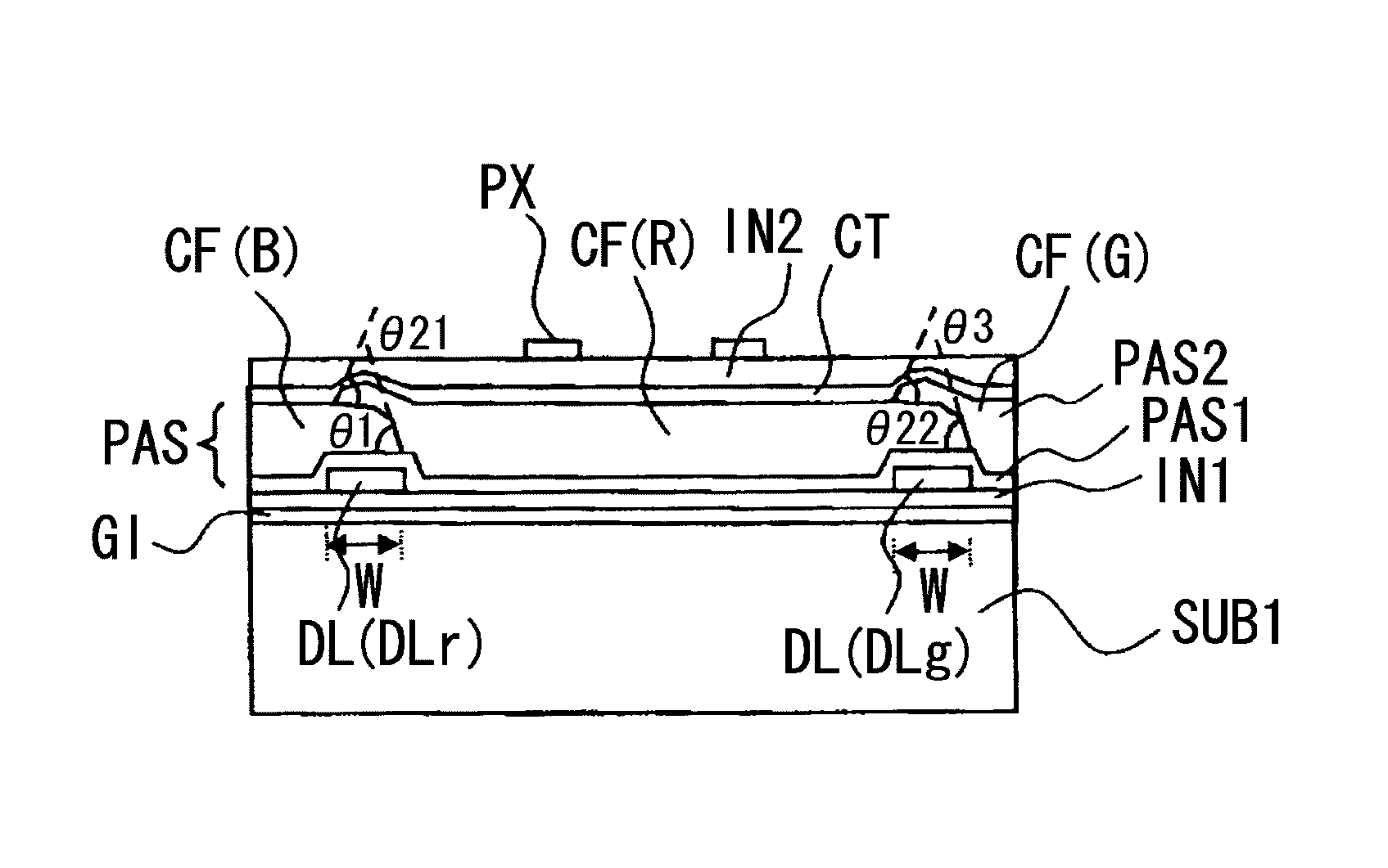
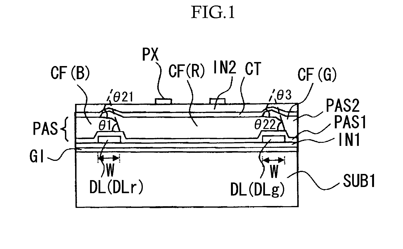
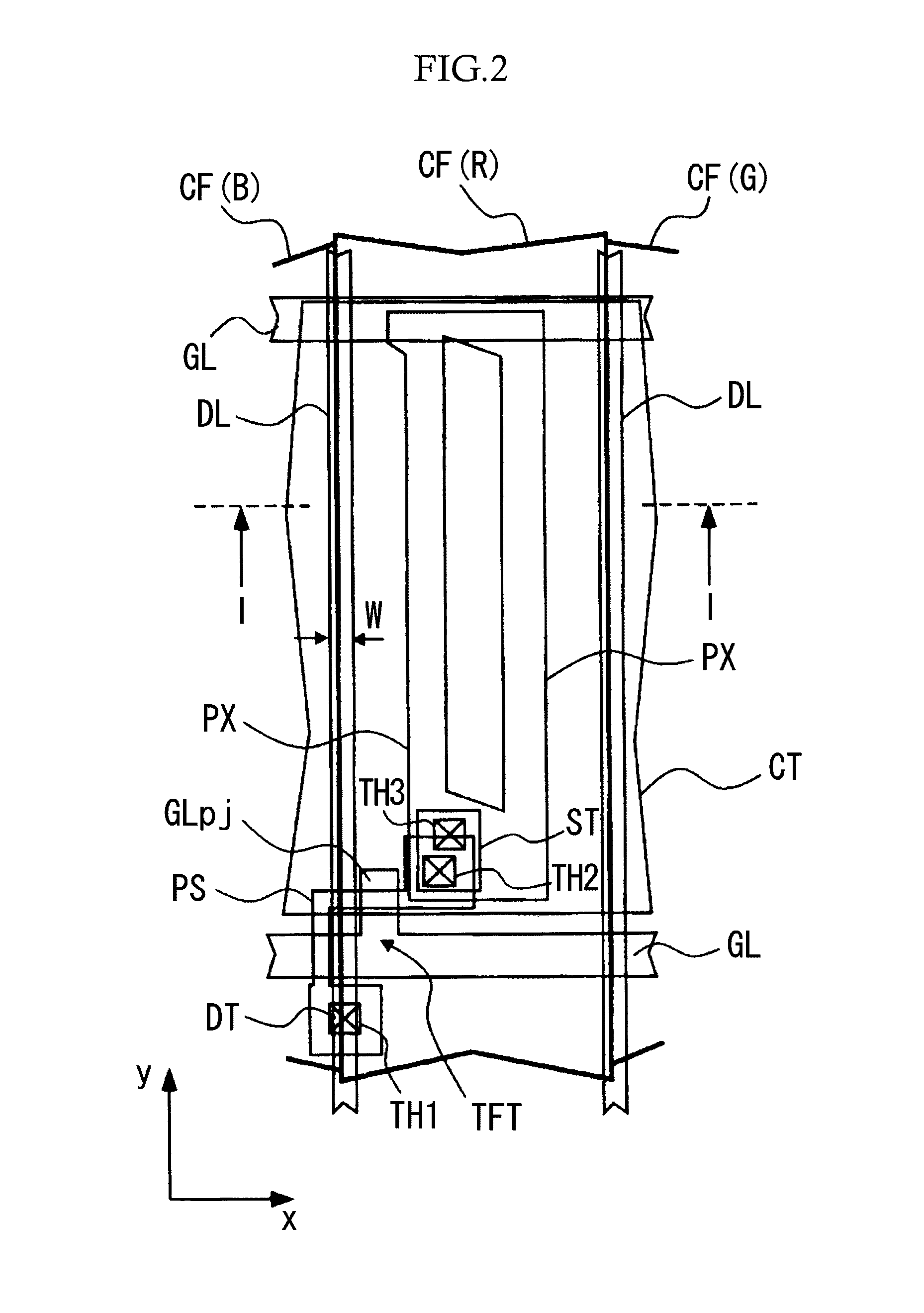
[0067]The liquid crystal display device according to the present invention has a pair of substrates that are positioned so as to face each other and sandwich liquid crystal, wherein gate signal lines made of a light blocking material which run in a first direction and are aligned in a second direction which crosses the above described first direction, and drain signal lines made of alight blocking material which run in the above described second direction and are aligned in the above described first direction, are formed on the surface of one of the two substrates, on the liquid crystal side, and thin film transistors which are turned on by a scanning signal through a gate signal line and pixel electrodes to which a video signal is supplied from a drain signal line through a thin film transistor when turned on are provided in pixel regions, pixel regions being defined as regions surrounded by two adjacent gate signal lines and two adjacent drain signal lines. Furthermore, each of th...
second embodiment
[0093]The second embodiment onward have more or less the structure shown in FIGS. 1 to 3, and therefore, the following descriptions are also based on Table 1.
[0094]The product for which the invention is used is the same as in the first embodiment. The order in which color filters CF for each pixel are layered in unit pixels is green (G), red (R) and blue (B). In the following descriptions, green is simply referred to as G, red is simply referred to as R, and blue is simply referred to as B for the sake of simplicity.
[0095]The density of the pigment in the color filters G is 20%, the film thickness is 4.0 μm, the relative dielectric constant is 3.6, and the angle of the taper is 45°. The density of the pigment in the color filters R is 10%, the film thickness is 4.0 μm, the relative dielectric constant is 3.0, and the angle of the taper is 45°. The density of the pigment in the color filters B is 10%, the film thickness is 4.0 μm, the relative dielectric constant is 3.3, and the angl...
third embodiment
[0096]The product for which the invention is used is the same as in the first embodiment. The order in which color filters for each pixel are layered in unit pixels is B, R and G.
[0097]The density of the pigment in the color filters B is 40%, the film thickness is 1.0 μm, the relative dielectric constant is 5.0, and the angle of the taper is 70°. The density of the pigment in the color filters R is 50%, the film thickness is 1.0 μm, the relative dielectric constant is 6.0, and the angle of the taper is 80°. The density of the pigment in the color filters G is 60%, the film thickness is 1.0 μm, the relative dielectric constant is 7.0, and the angle of the taper is 90°. The difference in thickness between the color filters for B and the color filters for R overlapping the color filters for B is 0.4 μm, the difference in thickness between the color filters for B and the color filters for G overlapping the color filters for B is 0.6 μm, and the difference in thickness between the color ...
PUM
| Property | Measurement | Unit |
|---|---|---|
| width | aaaaa | aaaaa |
| width | aaaaa | aaaaa |
| angle | aaaaa | aaaaa |
Abstract
Description
Claims
Application Information


