
PCB and processing method thereof

A processing method and sub-board technology are applied in the direction of multilayer circuit manufacturing, electrical connection of printed components, and structural connection of printed circuits, which can solve the problems of large aperture ratio, process complexity, high production cost, and large thickness. Small aperture ratio, reduce process complexity and production cost, and avoid the effect of excessive aperture ratio

Pending Publication Date: 2022-02-08
SPREADTRUM SEMICON (NANJING) CO LTD
View PDF0 Cites 0 Cited by
  • Summary
  • Abstract
  • Description
  • Claims
  • Application Information

AI Technical Summary

Problems solved by technology

[0004] However, in the existing technology, as the diameter of the PCB hole becomes smaller and smaller, the laminated PCB has more layers and a larger thickness, resulting in a very large aperture ratio, and the process complexity and production cost are getting higher and higher. , it is difficult to meet the needs of users

Method used


Image

  • PCB and processing method thereof
  • PCB and processing method thereof
  • PCB and processing method thereof

Examples


Embodiment Construction

[0030] In the prior art, as the diameter of the PCB hole becomes smaller and smaller, the laminated PCB has more layers and a larger thickness, resulting in a very large aperture ratio, increasing process complexity and production costs. Difficult to meet user needs.

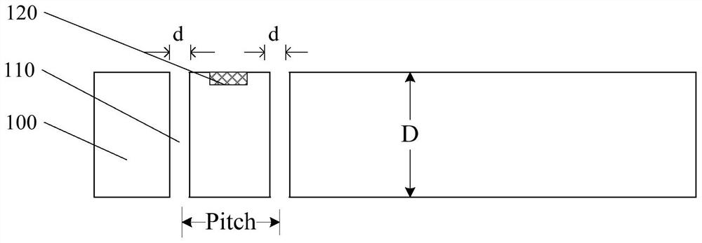
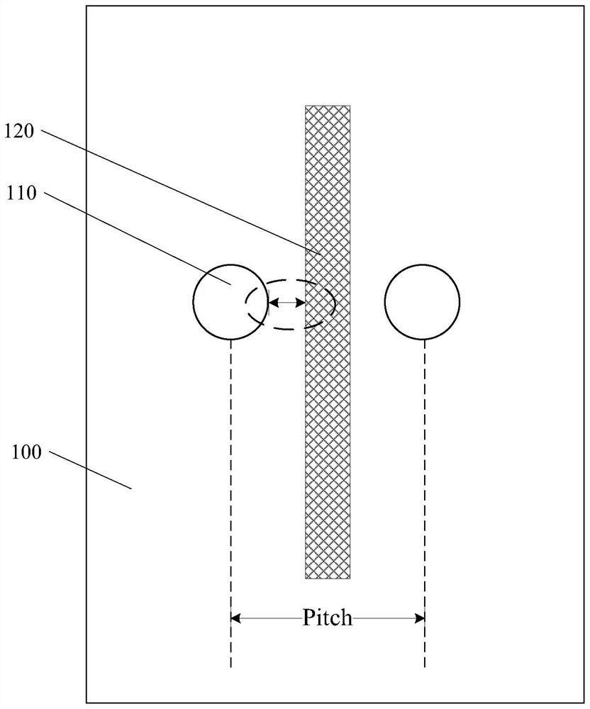
[0031] combined reference figure 1 and figure 2 , figure 1 is a schematic cross-sectional structure diagram of a PCB in the prior art, figure 2 It is a top view of a PCB in the prior art.

[0032] specifically, figure 1 The thickness of the PCB 100 shown is D, and a through hole 110 is processed on the PCB 100, the diameter of the through hole 110 is d.

[0033] It can be understood that as D becomes larger and d becomes smaller, the ratio of D to d (that is, the aperture ratio) also becomes larger.

[0034] Since in the PCB 100, it is necessary to reserve enough space between the through holes 100 to form the metal lines 120, it is necessary to limit the distance between the through holes 100, for examp...


PUM


Abstract

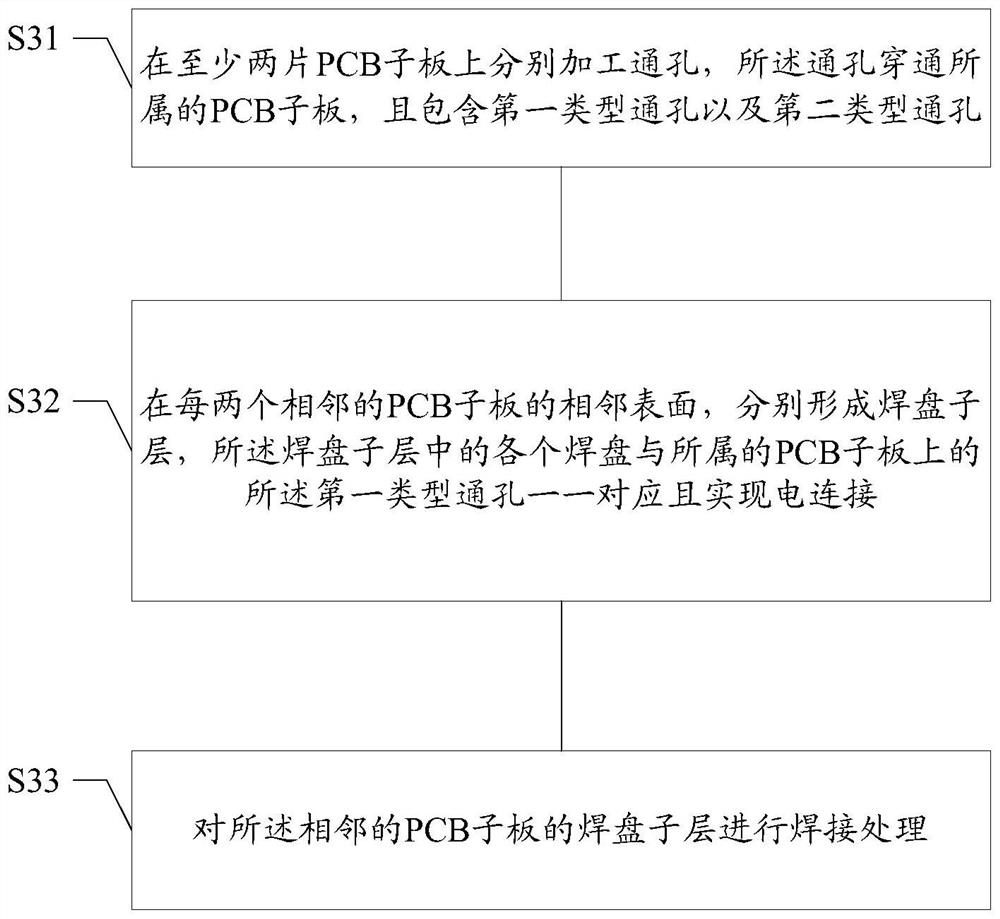
The invention discloses a PCB and a processing method thereof. The method comprises the steps of respectively processing through holes in at least two PCB sub-boards, wherein the through holes penetrate through the PCB sub-boards, and comprise a first type of through holes and a second type of through holes; forming welding plate sub-layers on the adjacent surfaces of every two adjacent PCB sub-boards respectively, wherein welding plates in the welding plate sub-layers correspond to the first type of through holes in the corresponding PCB sub-boards one to one and are electrically connected with the first type of through holes in the corresponding PCB sub-boards; and carrying out welding treatment on the welding plate sub-layers of the adjacent PCB sub-boards, wherein the first type of through holes are used for forming electric connection between adjacent PCB sub-boards, and the second type of through holes are used for forming electric connection inside and on the surface of the PCB sub-board to which the second type of through holes belong. According to the invention, the process complexity and the production cost can be effectively reduced, and the PCB sub-boards are combined through welding processing.

Description

technical field [0001] The invention relates to the technical field of communication, in particular to a PCB and a processing method thereof. Background technique [0002] With the rapid development of the performance of network products, the capacity requirements of the backplane channels used in network products are getting higher and higher. In order to meet the requirements of the channel capacity of the backplane, if the printed circuit board (PCB) used as the backplane is processed by ordinary single-sided crimping, not only the capacity of the backplane is difficult to meet the requirements, but also the PCB design layer The number is getting higher and higher, and the size design is getting bigger and bigger. At the same time, the increase in the number of layers leads to a corresponding increase in the board thickness, which brings great challenges to the conventional multi-layer PCB processing technology, mainly reflected in the large size, board thickness, general...

Claims


Application Information

Patent Timeline
Patent Type & Authority Applications(China)
IPC IPC(8): H05K3/00H05K3/46H05K1/11H05K1/14
CPCH05K3/0047H05K3/4623H05K3/4614H05K1/116H05K1/144
Inventor 唐甘霖林杰
Owner SPREADTRUM SEMICON (NANJING) CO LTD
Learn More