Display panel and display device including same

a display panel and display device technology, applied in the field of display panel and display device, can solve the problems of increasing the load on the gate line, difficult high-speed driving dulling of the potential of the gate line, etc., and achieve the effect of reducing the occurrence of display irregularities in the display region, and reducing the difference between luminances in the installation region and in the non-installation region

Active Publication Date: 2018-04-03
SHARP KK
View PDF10 Cites 3 Cited by
  • Summary
  • Abstract
  • Description
  • Claims
  • Application Information

AI Technical Summary

Benefits of technology

[0003]By providing the gate driver and the source driver on one side of the active matrix substrate, as is the case with JP-T-2004-538511 mentioned above, the frame can be narrowed on the other three sides. In Patent Document 1 mentioned above, however, the distance for which the gate lines are routed is longer than conventionally, which increases the loads on the gate lines. Consequently, potentials imparted to the gate lines are dulled, which makes high-speed driving of the gate lines difficult. The inventors of the present invention have invented an active matrix substrate characterized in that driving circuits that switch gate lines between selected and non-selected states are provided in a display region, and filed an application (Japanese Patent Application No. 2012-238805). By providing the driving circuits in the display region, the dullness of the gate lines is reduced, and at the same time, a narrower frame can be achieved. By providing the driving circuits in the display region, however, pixels where driving circuits are provided have aperture ratios smaller than those of pixels where driving circuits are not provided, thereby having different aperture ratios in the display region. This results in luminance differences in the display region, thereby causing display irregularities.
[0004]It is an object of the present invention to provide techniques for reducing occurrence of display irregularities in a display region even in a case where driving circuits that switch gate lines between selected and non-selected states are provided in the display region.
[0005]A display panel according to the first invention includes an active matrix substrate and a counter substrate, the active matrix substrate being provided with lines including a plurality of gate lines and a plurality of source lines, wherein the active matrix substrate includes, in a display region, a driving circuit provided with respect to each of the gate lines, the driving circuit switching the gate line between a selected state and a non-selected state. The display panel further includes, in a non-installation region where the driving circuit is not provided, an aperture ratio adjustment member that changes an aperture ratio in the non-installation region stepwise, in order to decrease a difference between a luminance in an installation region where the driving circuit is provided and a luminance in the non-installation region.
[0011]With the configuration of the present invention, even in a case where a driving circuit that switches a gate line between a selected state and a non-selected state is provided in a display region, the occurrence of display irregularities in the display region can be reduced.

Problems solved by technology

In Patent Document 1 mentioned above, however, the distance for which the gate lines are routed is longer than conventionally, which increases the loads on the gate lines.
Consequently, potentials imparted to the gate lines are dulled, which makes high-speed driving of the gate lines difficult.
This results in luminance differences in the display region, thereby causing display irregularities.

Method used


Image

  • Display panel and display device including same
  • Display panel and display device including same
  • Display panel and display device including same

Examples


embodiment 1

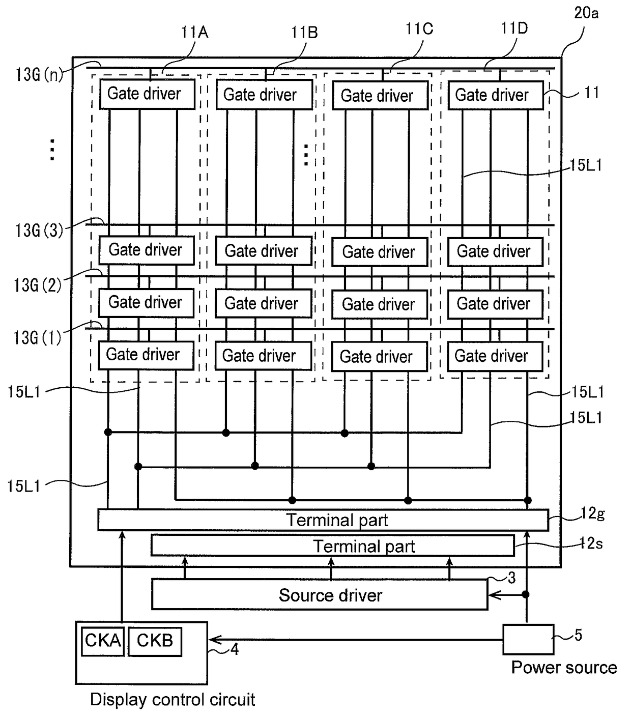
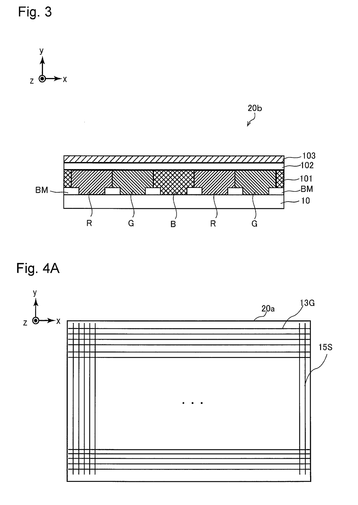
[0133]Described above as Embodiment 1 is an example in which the adjustment lines are provided in the gate driver non-installation region, at a ratio according to the difference between the aperture ratio in the gate driver installation region and the aperture ratio in the gate driver non-installation region. The following description describes, as the present embodiment, an example in which the aperture ratio in pixel region in the gate driver non-installation region is adjusted using the black matrix BM (aperture ratio adjustment member) on the counter substrate 20b. The following description describes the adjustment of the aperture ratio in the present embodiment, using the above-described example illustrated in FIG. 12.

[0134]As illustrated in FIGS. 7 and 9A to 9F mentioned above, each pixel region in the gate driver installation region is light-shielded by the light-shielded region BM. In FIGS. 7 and 9A to 9F, the light-shielded region BM includes the gate lines 13G, the source ...

embodiment 2

[0141]In Embodiment 2 described above, the gate driver non-installation region is light-shielded by the black matrix at a ratio according to the difference between the aperture ratio in the gate driver installation region and the aperture ratio in the gate driver non-installation region, in such a manner that, as the proximity to the gate driver installation region increases, the light-shielded region becomes larger. This reduces the luminance difference between the gate driver installation region and the gate driver non-installation region in the display region, thereby reducing display irregularities, as compared with the case where the light-shielded region BM in the gate driver non-installation region is not adjusted.

[0142]Described above as Embodiments 1 and 2 is an example in which light is emitted so that luminance of the backlight is approximately uniform on the display region. On the other hand, in the present embodiment, the luminance of the backlight is changed on the dis...


PUM

PropertyMeasurementUnit
widthaaaaaaaaaa
widthaaaaaaaaaa
colorsaaaaaaaaaa

Abstract

Provided is a display panel that reduces occurrence of display irregularities in a display region even in a case where driving circuits that switch gate lines between selected and non-selected states are provided in the display region. A display panel of the present invention includes an active matrix substrate and a counter substrate, the active matrix substrate being provided with a plurality of gate lines and a plurality of source lines. The active matrix substrate includes, in a display region, a driving circuit provided with respect to each of the gate lines, for switching the gate line between a selected state and a non-selected state. The display panel further includes, in a non-installation region where the driving circuit is not provided, an aperture ratio adjustment member that changes an aperture ratio in the non-installation region stepwise, in order to decrease a difference between a luminance in an installation region where the driving circuit is provided and a luminance in the non-installation region.

Description

TECHNICAL FIELD[0001]The present invention relates to a display panel and a display device including the same, and particularly relates to an arrangement of gate drivers.BACKGROUND ART[0002]Conventionally, a display panel in which a gate driver and a source driver are formed on adjacent two sides of an active matrix substrate has been known. Translation of PCT Application No. 2004-538511 (JP-T-2004-538511) discloses techniques for allowing row driving circuits that drive column address conductors to which data signals are supplied, and column driving circuits that drive row address conductors to which row selection signals are supplied, to be disposed on one side of a pixel element array. According to JP-T-2004-538511, with this configuration, peripheral regions around the pixel element array on a support body that holds the pixel element array or the like are not to be limited by these driving circuits.DISCLOSURE OF INVENTION[0003]By providing the gate driver and the source driver ...

Claims


Application Information

Patent Timeline
Patent Type & Authority Patents(United States)
IPC IPC(8): G09G5/02G09G5/10G06F3/038G09G5/00G09G3/36G02F1/1335G02F1/1345G02F1/1362
CPCG09G3/3655G02F1/13454G02F1/133512G02F1/136286G09G3/3607G09G5/10G09G3/3677G09G2320/0233G02F2201/52G09G2300/0452G09G2300/0465
Inventor YOSHIDA, HIDEFUMITANAKA, KOHHEI
Owner SHARP KK
Why Eureka
Try Eureka