Display panel and display device including same

a display panel and display device technology, applied in the field of display panel and display device, can solve the problems of increasing the load on the gate line, difficult high-speed driving dulling of the potential of the gate line, etc., and achieve the effect of reducing the occurrence of display irregularities in the display region, and reducing the difference between luminances in the installation region and in the non-installation region

Active Publication Date: 2016-07-21
SHARP KK
View PDF2 Cites 10 Cited by
  • Summary
  • Abstract
  • Description
  • Claims
  • Application Information

AI Technical Summary

Benefits of technology

[0010]The display device according to the sixth invention includes the display panel according to any one of the first to fifth inventions, and a light emission part that emits light from a side of the active matrix substrate of the display panel, in such a manner that a difference between a luminance in the installation region and a luminance in the non-installation region decreases.
[0011]With the configuration of the present invention, even in a case where a driving circuit that switches a gate line between a selected state and a non-selected state is provided in a display region, the occurrence of display irregularities in the display region can be reduced.

Problems solved by technology

In Patent Document 1 mentioned above, however, the distance for which the gate lines are routed is longer than conventionally, which increases the loads on the gate lines.
Consequently, potentials imparted to the gate lines are dulled, which makes high-speed driving of the gate lines difficult.
This results in luminance differences in the display region, thereby causing display irregularities.

Method used


Image

  • Display panel and display device including same
  • Display panel and display device including same
  • Display panel and display device including same

Examples


embodiment 1

Configuration of Liquid Crystal Display Device

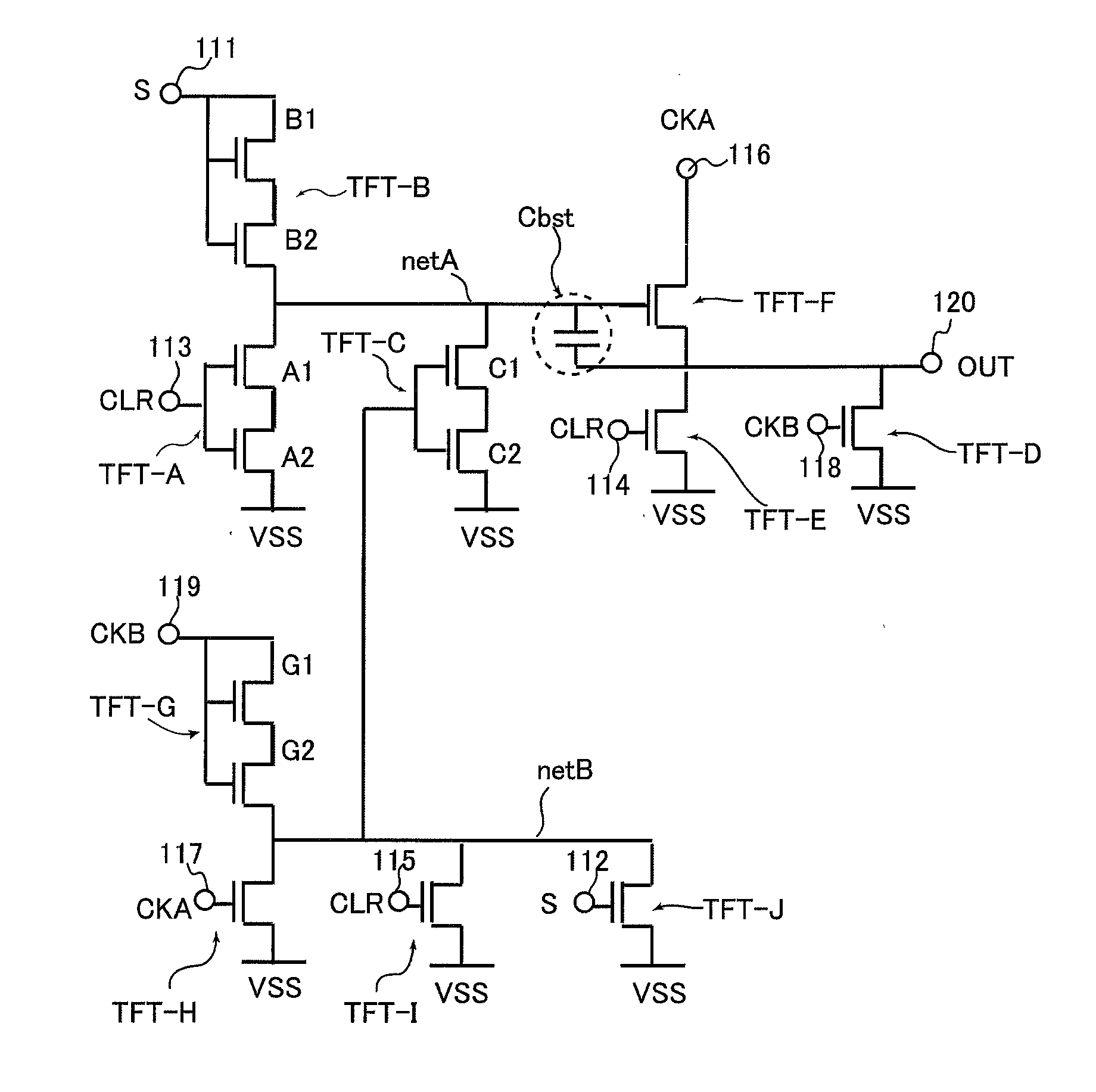
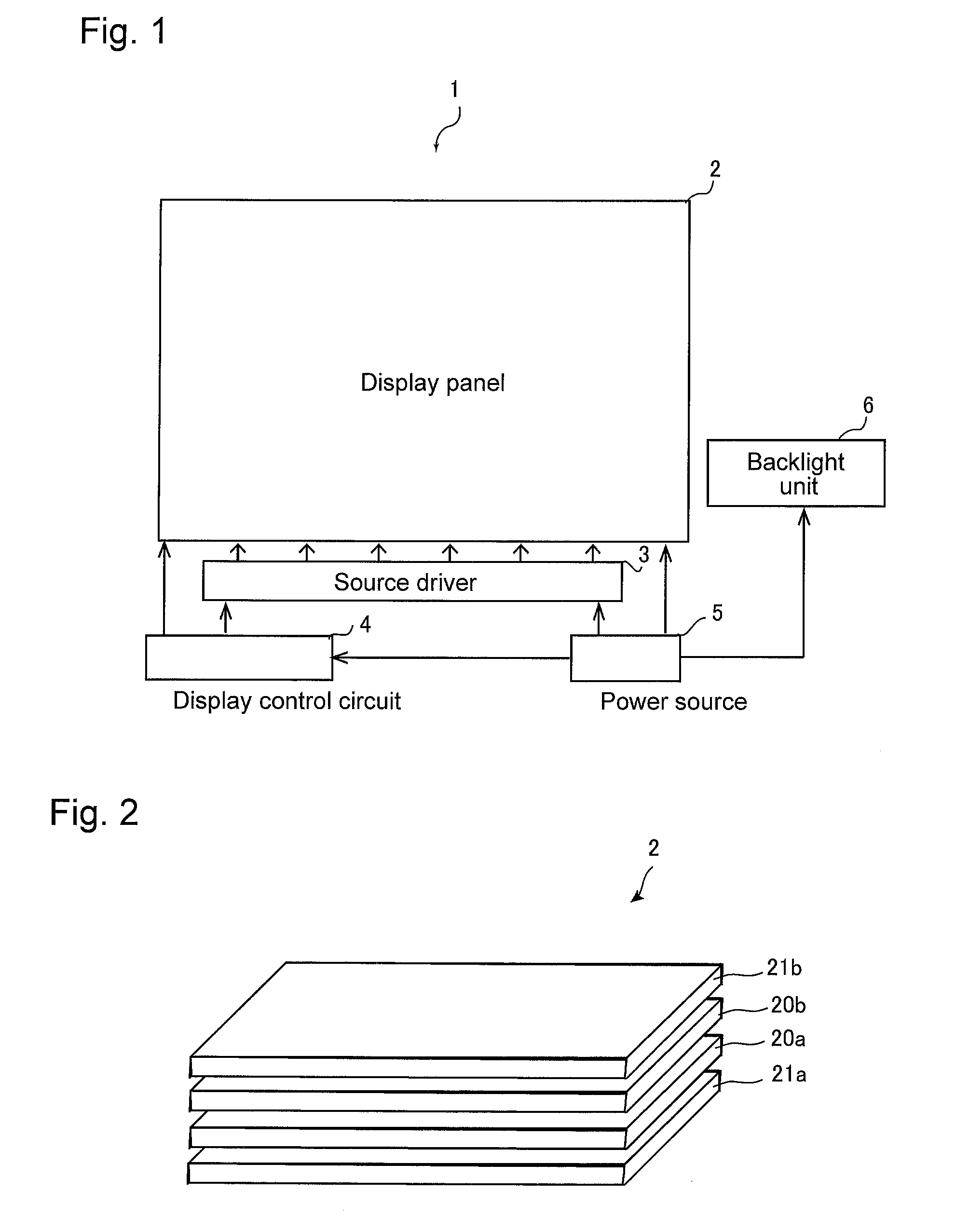
[0060]FIG. 1 is a schematic diagram illustrating a schematic configuration of a liquid crystal display device according to the present embodiment. A liquid crystal display device 1 includes a display panel 2, a source driver 3, a display control circuit 4, a power source 5, and a backlight unit 6. The display panel 2 is electrically connected with the source driver 3 formed on a flexible substrate. The display control circuit 4 is electrically connected with the display panel 2, the source driver 3, and the power source 5. The display control circuit 4 outputs control signals to the source driver 3, and driving circuits formed in the display panel 2 (hereinafter referred to as “gate drivers”), which are to be described below. The control signals include a reset signal (CLR), clock signals (CKA, CKB), data signals, and the like for displaying images on the display panel 2. The power source 5 is electrically connected with the display pane...

embodiment 2

[0133]Described above as Embodiment 1 is an example in which the adjustment lines are provided in the gate driver non-installation region, at a ratio according to the difference between the aperture ratio in the gate driver installation region and the aperture ratio in the gate driver non-installation region. The following description describes, as the present embodiment, an example in which the aperture ratio in pixel region in the gate driver non-installation region is adjusted using the black matrix BM (aperture ratio adjustment member) on the counter substrate 20b. The following description describes the adjustment of the aperture ratio in the present embodiment, using the above-described example illustrated in FIG. 12.

[0134]As illustrated in FIGS. 7 and 9A to 9F mentioned above, each pixel region in the gate driver installation region is light-shielded by the light-shielded region BM. In FIGS. 7 and 9A to 9F, the light-shielded region BM includes the gate lines 13G, the source ...

embodiment 3

[0142]Described above as Embodiments 1 and 2 is an example in which light is emitted so that luminance of the backlight is approximately uniform on the display region. On the other hand, in the present embodiment, the luminance of the backlight is changed on the display region, depending differences in aperture ratios in the display region. The following description describes this example.

[0143]In an example described above as Embodiments 1 and 2, the gate driver groups 11A, 11B, 11C, and 11D are provided in the display region, but as the present embodiment, for convenience of explanation, a configuration is described in which the gate driver groups 11A, 11D are provided in the display region, as illustrated in FIG. 18. In addition, in FIG. 18, the gate driver non-installation region S20 between the gate driver installation region in the gate driver group 11A and the gate driver installation region in the gate driver group 11D is, as is the case with Embodiment 1 or 2 described abov...


PUM


Abstract

Provided is a display panel that reduces occurrence of display irregularities in a display region even in a case where driving circuits that switch gate lines between selected and non-selected states are provided in the display region. A display panel of the present invention includes an active matrix substrate and a counter substrate, the active matrix substrate being provided with a plurality of gate lines and a plurality of source lines. The active matrix substrate includes, in a display region, a driving circuit provided with respect to each of the gate lines, for switching the gate line between a selected state and a non-selected state. The display panel further includes, in a non-installation region where the driving circuit is not provided, an aperture ratio adjustment member that changes an aperture ratio in the non-installation region stepwise, in order to decrease a difference between a luminance in an installation region where the driving circuit is provided and a luminance in the non-installation region.

Description

TECHNICAL FIELD[0001]The present invention relates to a display panel and a display device including the same, and particularly relates to an arrangement of gate drivers.BACKGROUND ART[0002]Conventionally, a display panel in which a gate driver and a source driver are formed on adjacent two sides of an active matrix substrate has been known. Translation of PCT Application No. 2004-538511 (JP-T-2004-538511) discloses techniques for allowing row driving circuits that drive column address conductors to which data signals are supplied, and column driving circuits that drive row address conductors to which row selection signals are supplied, to be disposed on one side of a pixel element array. According to JP-T-2004-538511, with this configuration, peripheral regions around the pixel element array on a support body that holds the pixel element array or the like are not to be limited by these driving circuits.DISCLOSURE OF INVENTION[0003]By providing the gate driver and the source driver ...

Claims


Application Information

Patent Timeline
Patent Type & Authority Applications(United States)
IPC IPC(8): G09G3/36G09G5/10
CPCG09G3/3655G09G3/3607G09G2320/0233G09G2300/0452G09G2300/0465G09G5/10G02F1/13454G02F1/136286G09G3/3677G02F1/133512G02F2201/52
Inventor YOSHIDA, HIDEFUMITANAKA, KOHHEI
Owner SHARP KK
Why Eureka
Try Eureka