Metallic electrode forming method and semiconductor device having metallic electrode

a technology of metal electrodes and forming methods, which is applied in the testing/measurement of individual semiconductor devices, semiconductor/solid-state devices, instruments, etc., can solve the problems of product yield degradation and intensification of surface roughness of protective films having undergone cutting work, so as to increase surface roughness and reduce the effect of surface roughness

Inactive Publication Date: 2008-09-11
DENSO CORP
View PDF11 Cites 19 Cited by
  • Summary
  • Abstract
  • Description
  • Claims
  • Application Information

AI Technical Summary

Benefits of technology

[0014]When the semiconductor substrate is adsorbed or secured to the adsorption stage, although a difference between concave and convex parts of the surface portion increases while reflecting the back-side shape thereof, the difference between the concave and convex parts of the surface portion can be decreased. Moreover, the distance between the cutting plane and surface portion can be confined to the predetermined range. Consequently, since the precision in cutting work can be improved, a product yield in formation of metallic electrodes can be improved.
[0021]In the semiconductor device, a variance in the thickness of a portion cut through cutting work is smaller than the difference between concave and convex parts of the back side of the semiconductor substrate. Consequently, all area is satisfied with a requested degree of precision in a magnitude of cutting. A product yield can be improved.
[0027]In the above method, the flatness of the surface of the metallic film is improved. Moreover, even when the semiconductor substrate is adsorbed or secured during cutting work, the surface of the metallic film will not be shaped to have large irregularities while reflecting the original irregular shape of the back side. Namely, the difference between concave and convex parts of the surface of the metallic film is decreased, and the distance between a cutting plane for the cutting work and the surface of the metallic film is confined to a predetermined range. Consequently, since the precision in cutting work can be improved, a product yield in formation of metallic electrodes can be improved.
[0031]In the above method, the flatness of the surface of the metallic film is improved. Even when the semiconductor substrate is adsorbed or secured during cutting work, the surface of the metallic film will not be shaped to have large irregularities while reflecting the original irregular shape of the back side. Namely, the difference between concave and convex parts of the surface of the metallic film is decreased, and the distance between a cutting plane for the cutting work and the surface of the metallic film is confined to a predetermined range. Consequently, since the precision in cutting work can be improved, a product yield in formation of metallic electrodes can be improved.
[0035]In the above method, an area where the protective film which has been cut by the first blade portion and whose surface has been plucked to intensify the surface roughness is bared can be cut using the second blade portion during cutting to be performed after the cutting tool is moved by the designated pitch. Consequently, the surface roughness of the protective film having undergone cutting work can be diminished.

Problems solved by technology

This poses a problem in that a product yield is degraded.
This poses a problem in that the surface roughness of the protective film having undergone cutting work is intensified.

Method used


Image

  • Metallic electrode forming method and semiconductor device having metallic electrode
  • Metallic electrode forming method and semiconductor device having metallic electrode
  • Metallic electrode forming method and semiconductor device having metallic electrode

Examples


first embodiment

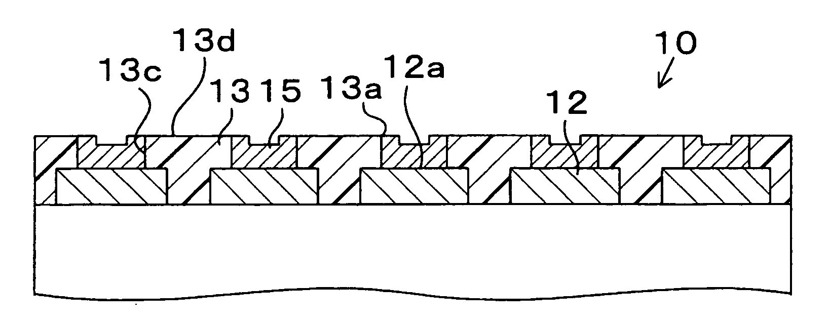
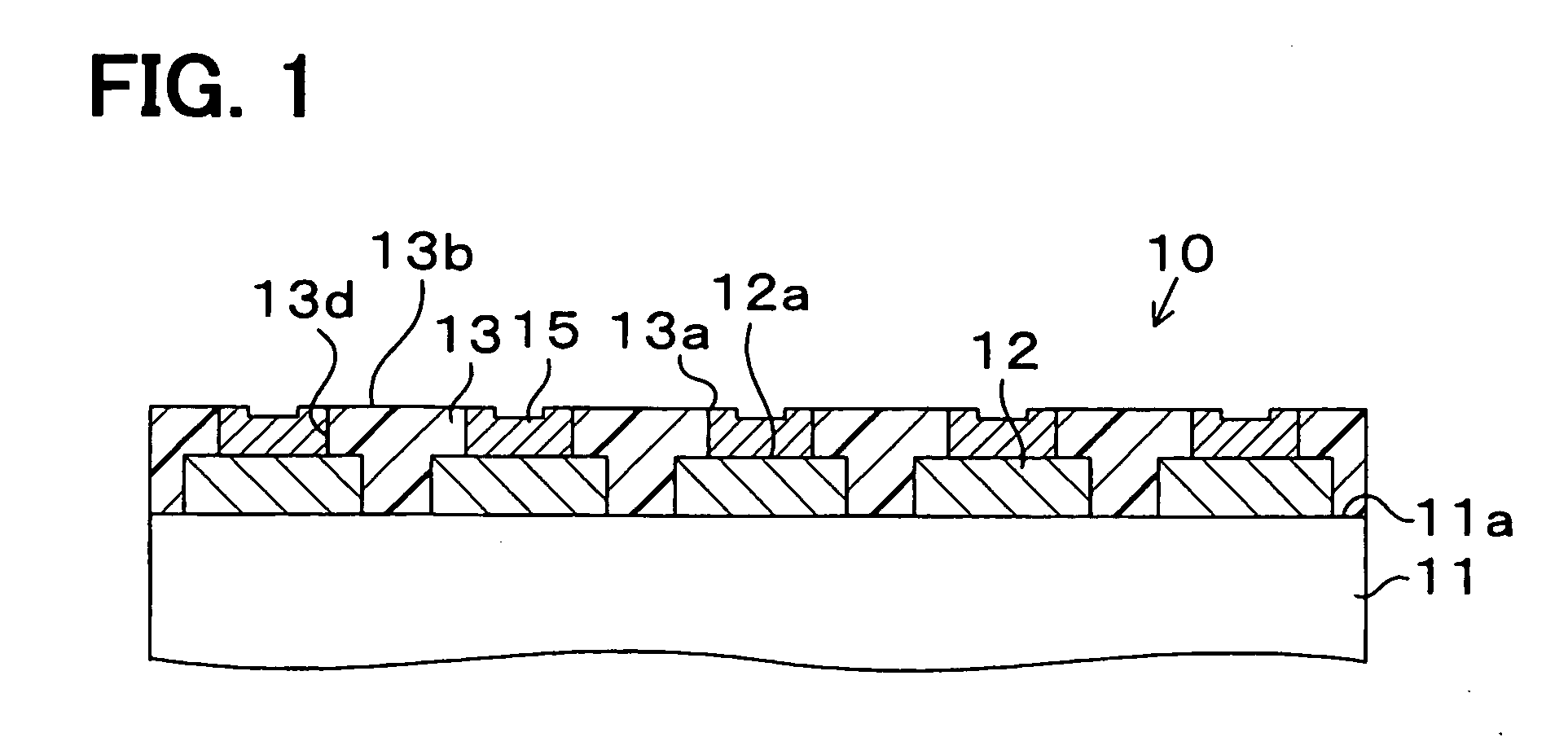
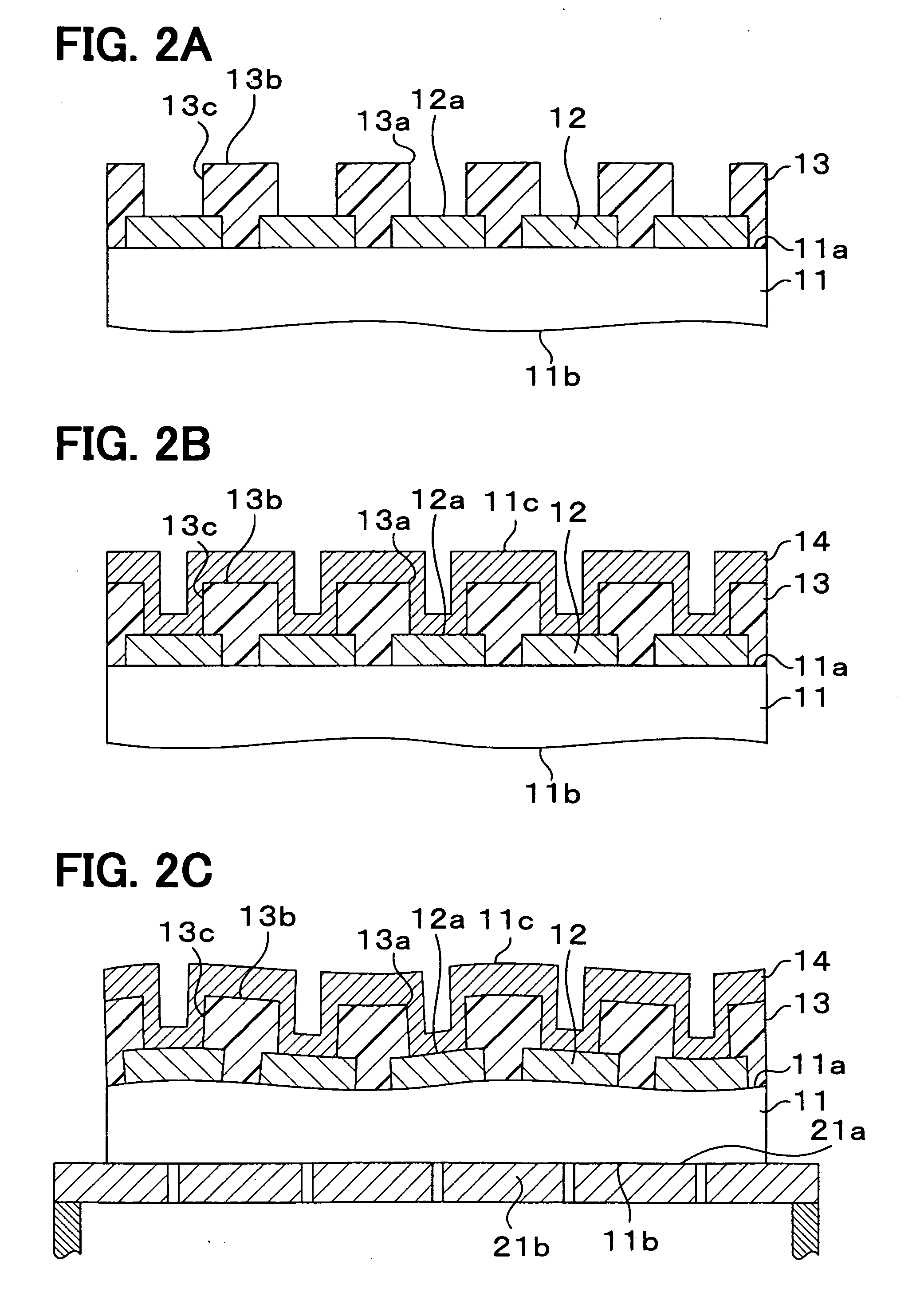
[0064]Referring to the drawings, the first embodiment of a metallic electrode forming method for semiconductor devices and a semiconductor device in accordance with the present invention will be described below. FIG. 1 is a sectional explanatory view of a semiconductor device having metallic electrodes formed thereon according to the metallic electrode forming method of the first embodiment. FIG. 2A to FIG. 4B show steps included in the metallic electrode forming method. FIG. 5A and FIG. 5B are explanatory views of a surface shape control apparatus. FIG. 5A is a sectional view, and FIG. 5B is a plan explanatory view of the surface shape control apparatus seen from a semiconductor substrate side. FIG. 6A to FIG. 6C are explanatory diagrams presenting an example of surface shape control for the semiconductor substrate. FIG. 6A is a profile of thicknesses of the semiconductor substrate detected during adsorption, FIG. 6B is a profile of displacements applied by a deformation unit, and ...

second embodiment

[0117]The second embodiment of a metallic electrode forming method for semiconductor devices and a semiconductor device in accordance with the present invention will be described below with reference to the drawings. Herein, a description will be made on the assumption that Au electrodes are adopted as electrodes which bring power elements such as bipolar transistors or transverse diffusion transistors (LDMOS) into contact with an external substrate. FIG. 8A to FIG. 10 are sectional explanatory diagrams concerning an electrode forming method for semiconductor devices of the second embodiment.

[0118]Incidentally, the same reference numerals will be assigned to components identical to those of the first embodiment. An iterative description will be omitted.

[0119]A method of forming the metallic electrodes 15 will be described below.

[0120]First, as shown in FIG. 8A, the semiconductor substrate 11 having power elements, which are not shown, formed thereon is prepared, and patterned accord...

third embodiment

[0143]Referring to the drawings, the third embodiment of a metallic electrode forming method for semiconductor devices in accordance with the present invention will be described below. FIG. 1 is a sectional explanatory view of a semiconductor device having metallic electrodes formed according to the metallic electrode forming method of the third embodiment. FIG. 13A to FIG. 15B show steps included in the metallic electrode forming method. FIG. 16A and FIG. 16B are explanatory views presenting a variant of a method of pouring a filler for formation of a flat portion.

[0144]A semiconductor device 10 adapted to a power card or the like is formed using a semiconductor substrate 11, which is made of silicon or the like, as a body. Bed electrodes 12 that are element electrodes are formed on the principal side 11a of the semiconductor substrate 11 using pure aluminum (Al) or an aluminum alloy such as an aluminum-silicon (Al—Si) alloy or an aluminum-silicon-copper (Al—Si—Cu) alloy.

[0145]A pr...


PUM

PropertyMeasurementUnit
cutting depthaaaaaaaaaa
thicknessaaaaaaaaaa
surface roughnessaaaaaaaaaa

Abstract

A metallic electrode forming method includes: forming a bed electrode on a substrate; forming a protective film with an opening on the bed electrode to expose the bed electrode from the opening; forming a metallic film covering the protective film and the opening; mounting the substrate on an adsorption stage, and measuring a surface shape of the metallic film by a surface shape measuring means; deforming the substrate by a deforming means so that a difference between the principal surface and a cutting surface is within a predetermined range; measuring a surface shape of the principal surface, and determining whether the difference is within a predetermined range; and cutting the substrate along with the cutting surface so that the metallic film is patterned to be a metallic electrode.

Description

CROSS REFERENCE TO RELATED APPLICATIONS[0001]This application is based on Japanese Patent Applications No. 2007-55982 filed on Mar. 6, 2007, No. 2007-194016 filed on Jul. 26, 2007, No. 2007-222762 filed on Aug. 29, 2007 and No. 2007-337039 filed on Dec. 27, 2007, the disclosures of which are incorporated herein by reference.FIELD OF THE INVENTION[0002]The present invention relates to a metallic electrode forming method and a semiconductor device having a metallic electrode.BACKGROUND OF THE INVENTION[0003]In recent years, there has been a demand for inexpensive formation of metallic electrodes, which are used for solder joint or the like, on a circuit surface formed on a semiconductor substrate.[0004]In response to the demand, as a technology for forming metallic electrodes without the necessity of including a photolithography step in patterning, a patent document 1 (JP-A-2006-186304) has disclosed a technology for forming metallic electrodes that is implemented in a process of fabr...

Claims


Application Information

Patent Timeline
Patent Type & Authority Applications(United States)
IPC IPC(8): H01L21/66H01L23/498H01L21/78
CPCH01L21/7684H01L22/12H01L2924/1305H01L2924/0001H01L2224/131H01L2924/014H01L2924/01074H01L24/11H01L24/13H01L2224/13099H01L2924/01013H01L2924/01022H01L2924/01029H01L2924/01049H01L2924/01052H01L2924/01059H01L2924/01078H01L2924/01079H01L2924/01082H01L2924/04941H01L2924/19042H01L2924/01006H01L2924/01023H01L2924/01033H01L2924/01068H01L2924/00H01L2224/05022H01L2224/05001H01L2224/05572H01L2224/05647H01L2224/05666H01L2924/00014H01L2224/05686H01L24/05H01L24/03H01L2224/05099
Inventor TOMISAKA, MANABUKOJIMA, HISATOSHINIIMI, AKIHIRO
Owner DENSO CORP
Why Eureka
Try Eureka