Semiconductor substrate and method for producing semiconductor substrate

a semiconductor substrate and semiconductor technology, applied in the direction of crystal growth process, polycrystalline material growth, chemically reactive gas growth process, etc., can solve the problems of difficult to form a single crystal ingot, difficult to form a sic substrate with a large diameter and few crystal defects by sublimation method, and high price of the substra

Active Publication Date: 2015-03-24
SEIKO EPSON CORP
View PDF42 Cites 0 Cited by
  • Summary
  • Abstract
  • Description
  • Claims
  • Application Information

AI Technical Summary

Benefits of technology

[0008]An advantage of some aspects of the invention is to provide a semiconductor substrate capable of forming a high-quality single crystal silicon carbide film with few crystal defects and a method for producing such a semiconductor substrate are provided.

Problems solved by technology

Since the crystal formation temperature of SiC is higher than that of Si, it is difficult to form a single crystal ingot by a pulling method from a liquid phase, and a single crystal ingot is formed by a sublimation method.
However, it is very difficult to form a SiC substrate having a large diameter and few crystal defects by a sublimation method.
Therefore, the diameter of a currently available SiC substrate is from 3 to 4 inches, and also the price thereof is very high.
Further, Si and 3C-SiC are also different in thermal expansion coefficient, and therefore, it is difficult to obtain a high-quality epitaxial film with few crystal defects.
However, in a process in which single crystal silicon carbide is epitaxially grown and the temperature is returned to room temperature, it is difficult to suppress stress caused by a difference in thermal expansion coefficient between the substrate and the single crystal silicon carbide.
If stress is caused by a difference in thermal expansion coefficient, crystal defects may occur in a single crystal silicon carbide film.

Method used


Image

  • Semiconductor substrate and method for producing semiconductor substrate
  • Semiconductor substrate and method for producing semiconductor substrate
  • Semiconductor substrate and method for producing semiconductor substrate

Examples


first embodiment

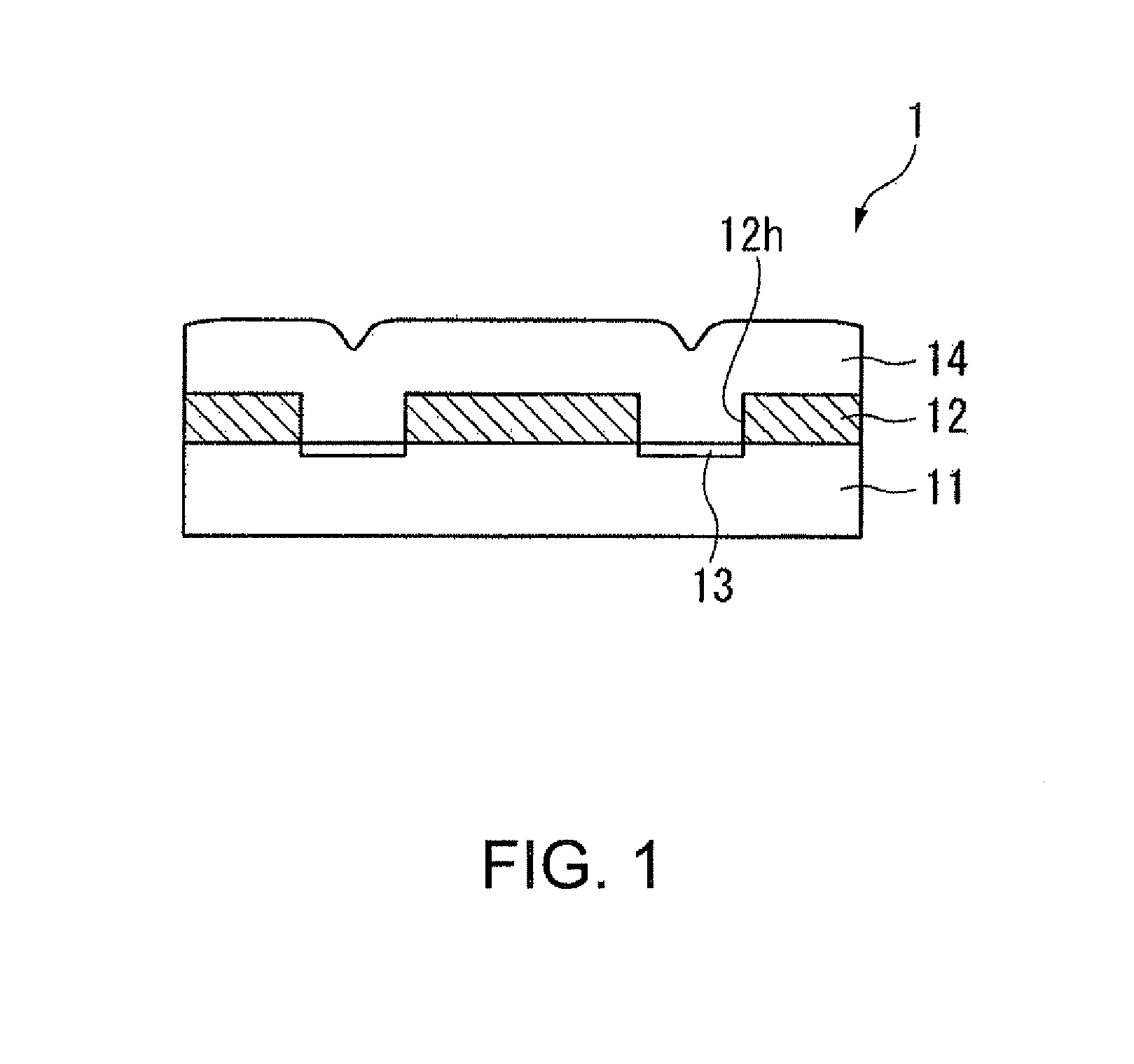
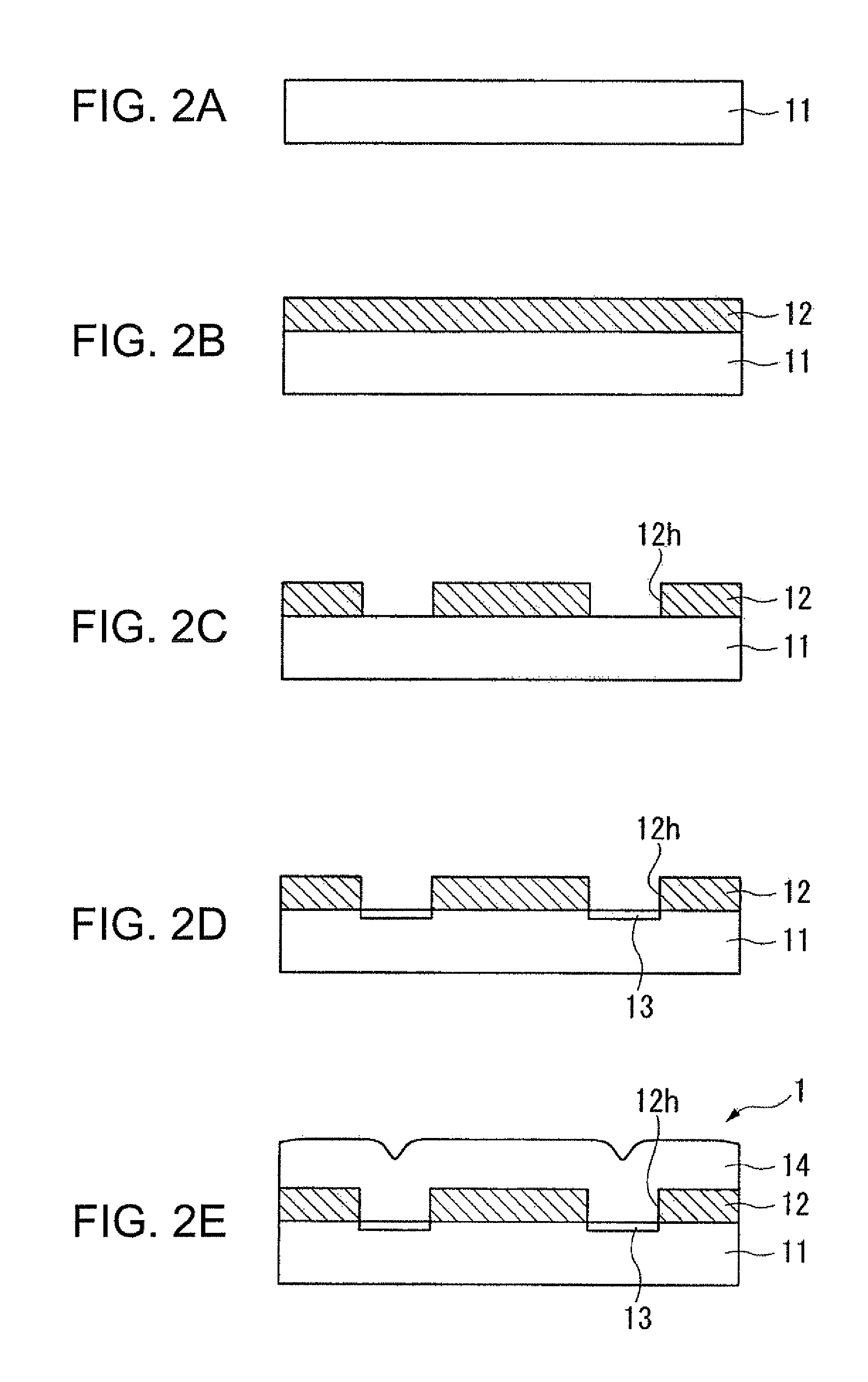
[0038]FIG. 1 is a schematic view showing a structure of a semiconductor substrate 1 according to a first embodiment of the invention.

[0039]As shown in FIG. 1, the semiconductor substrate 1 is provided with: single crystal silicon 11; a mask material 12 formed on a surface of the single crystal silicon 11 and having openings 12h; silicon carbide films 13 formed on portions of the single crystal silicon 11 exposed in the openings 12h; and a single crystal silicon carbide film 14 formed so as to cover the silicon carbide films 13 exposed in the openings 12h and the mask material 12.

[0040]The single crystal silicon 11 is formed by, for example, slicing a silicon single crystal ingot pulled by a Czochralski (CZ) method, followed by polishing. The surface of the single crystal silicon 11 forms a crystal plane represented by a Miller index (100). Further, an offset substrate in which a crystal axis of the crystal plane is tilted by several degrees may be used.

[0041]In this embodiment, a si...

second embodiment

[0086]FIG. 6 is a schematic view showing a structure of a semiconductor substrate 2 according to a second embodiment of the invention.

[0087]As shown in FIG. 6, the semiconductor substrate 2 is provided with: single crystal silicon 21; a silicon carbide film 22 formed on a surface of the single crystal silicon 21; a mask material 23 formed on a surface of the silicon carbide film 22 and having openings 23h; and a single crystal silicon carbide film 24 formed so as to cover the silicon carbide film 22 exposed in the openings 23h and the mask material 23.

[0088]The single crystal silicon 21 is formed by, for example, slicing a silicon single crystal ingot pulled by a Czochralski (CZ) method, followed by polishing. The surface of the single crystal silicon 21 forms a crystal plane represented by a Miller index (100).

[0089]The silicon carbide film 22 is formed on a surface of the single crystal silicon 21. The silicon carbide film 22 is a silicon carbide (3C-SiC) single crystal or polycry...

first modification example

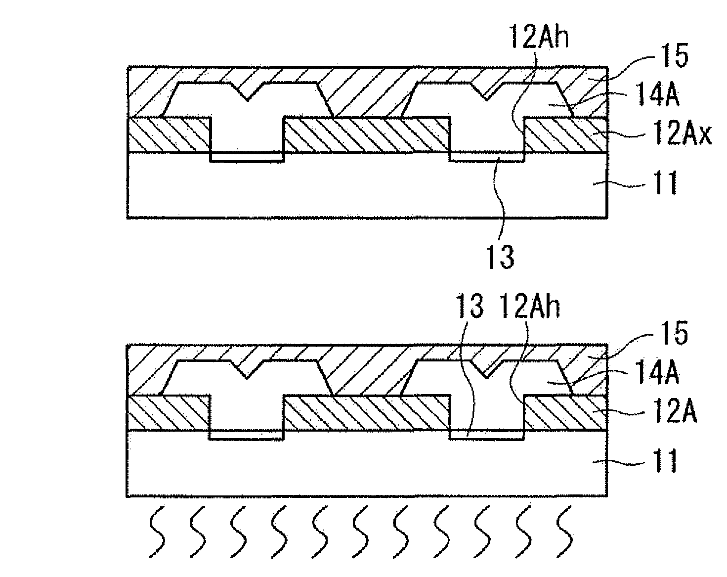
[0105]FIGS. 8A to 8C and FIGS. 9A to 9E are process drawings showing a first modification example of the method for producing a semiconductor substrate according to the second embodiment.

[0106]First, single crystal silicon 21 is provided and the single crystal silicon is placed in a vacuum chamber. Then, a heat treatment is performed in a vacuum atmosphere under the conditions that a treatment temperature is 750° C. and a treatment time is 5 minutes. Subsequently, the treatment temperature is decreased to 600° C.

[0107]Subsequently, the substrate temperature is adjusted to a temperature in a range of 600 to 800° C., and a raw material gas (a carbon material gas) for a silicon carbide film 22 is introduced into the chamber while maintaining this adjusted substrate temperature. By doing this, the silicon carbide film 22 is formed on a surface of the single crystal silicon 21 (a first step, see FIG. 8A).

[0108]Subsequently, a silicon oxide film 23Ax is formed on a surface of the silicon ...


PUM

PropertyMeasurementUnit
temperatureaaaaaaaaaa
diameteraaaaaaaaaa
lattice constantsaaaaaaaaaa

Abstract

A semiconductor substrate includes: single crystal silicon; a mask material formed on a surface of the single crystal silicon and having an opening; a silicon carbide film formed on a portion exposed in the opening of the single crystal silicon; and a single crystal silicon carbide film formed so as to cover the silicon carbide film and the mask material. The mask material has a viscosity of 105 Pa·S or more and 1014.5 Pa·S or less in a temperature range of 950 to 1400° C.

Description

BACKGROUND[0001]1. Technical Field[0002]The present invention relates to a semiconductor substrate and a method for producing a semiconductor substrate.[0003]2. Related Art[0004]Silicon carbide (SiC) which is a wide band gap semiconductor has a band gap twice or more than twice as wide as that of silicon (Si) in the related art and has attracted attention as a material for high-pressure resistant devices. Since the crystal formation temperature of SiC is higher than that of Si, it is difficult to form a single crystal ingot by a pulling method from a liquid phase, and a single crystal ingot is formed by a sublimation method. However, it is very difficult to form a SiC substrate having a large diameter and few crystal defects by a sublimation method. Therefore, the diameter of a currently available SiC substrate is from 3 to 4 inches, and also the price thereof is very high.[0005]As the types of SiC, there are cubic silicon carbide (3C-SiC), hexagonal silicon carbide (4H-SiC, 6H-SiC)...

Claims


Application Information

Patent Timeline
Patent Type & Authority Patents(United States)
IPC IPC(8): H01L29/16C30B25/04C30B29/36C30B25/18H01L21/02
CPCH01L21/02529H01L21/02381H01L21/0262H01L21/02639H01L21/02647C30B25/04C30B25/183C30B29/36
Inventor WATANABE, YUKIMUNE
Owner SEIKO EPSON CORP
Why Eureka
Try Eureka