Silicon carbide epitaxial wafer manufacturing method, silicon carbide semiconductor device manufacturing method and silicon carbide epitaxial wafer manufacturing apparatus

a silicon carbide and epitaxial wafer technology, applied in the direction of polycrystalline material growth, chemically reactive gas growth, crystal growth process, etc., can solve the problems of reducing device yield, generating leak current, and forming carbide particles, so as to achieve fewer crystal defects

Inactive Publication Date: 2019-08-06
MITSUBISHI ELECTRIC CORP
View PDF7 Cites 0 Cited by
  • Summary
  • Abstract
  • Description
  • Claims
  • Application Information

AI Technical Summary

Benefits of technology

[0007]In view of the above-described problems, an object of the present invention is to provide a silicon carbide epitaxial wafer manufacturing method, a silicon carbide semiconductor device manufacturing method and a silicon carbide epitaxial wafer manufacturing apparatus capable of manufacturing a silicon carbide epitaxial wafer having fewer crystal defects.
[0009]In the present invention, silicon carbide attached to the inner wall surfaces of the growth furnace is stabilized by being nitrided before epitaxial growth is performed, thus enabling inhibition of generation of silicon carbide particles. Manufacturing of a silicon carbide epitaxial wafer having fewer crystal defects due to silicon carbide particles is enabled thereby.

Problems solved by technology

If defects exist in the silicon carbide epitaxial wafer due to faults in the silicon carbide substrate and the silicon carbide epitaxially grown layer during growth, a place where a high voltage cannot be maintained can occur locally, resulting in generation of a leak current.
Silicon carbide is also attached to inner wall surfaces of a growth furnace, and this silicon carbide tends to form silicon carbide particles because of the brittleness of its structure.
If silicon carbide particles are attached to the surface of a silicon carbide wafer, crystal defects such as downfalls and triangular defects are generated from the places where the silicon carbide particles are attached, resulting in a reduction in device yield.
In a case where SiO2 film or Si3N4 film is formed on the surface of a susceptor, and where silicon carbide is epitaxially grown on the SiO2 film or Si3N4 film, the adhesion between silicon carbide and the film is so low that silicon carbide particles can easily be generated and crystal defects are increased.

Method used


Image

  • Silicon carbide epitaxial wafer manufacturing method, silicon carbide semiconductor device manufacturing method and silicon carbide epitaxial wafer manufacturing apparatus
  • Silicon carbide epitaxial wafer manufacturing method, silicon carbide semiconductor device manufacturing method and silicon carbide epitaxial wafer manufacturing apparatus
  • Silicon carbide epitaxial wafer manufacturing method, silicon carbide semiconductor device manufacturing method and silicon carbide epitaxial wafer manufacturing apparatus

Examples


first embodiment

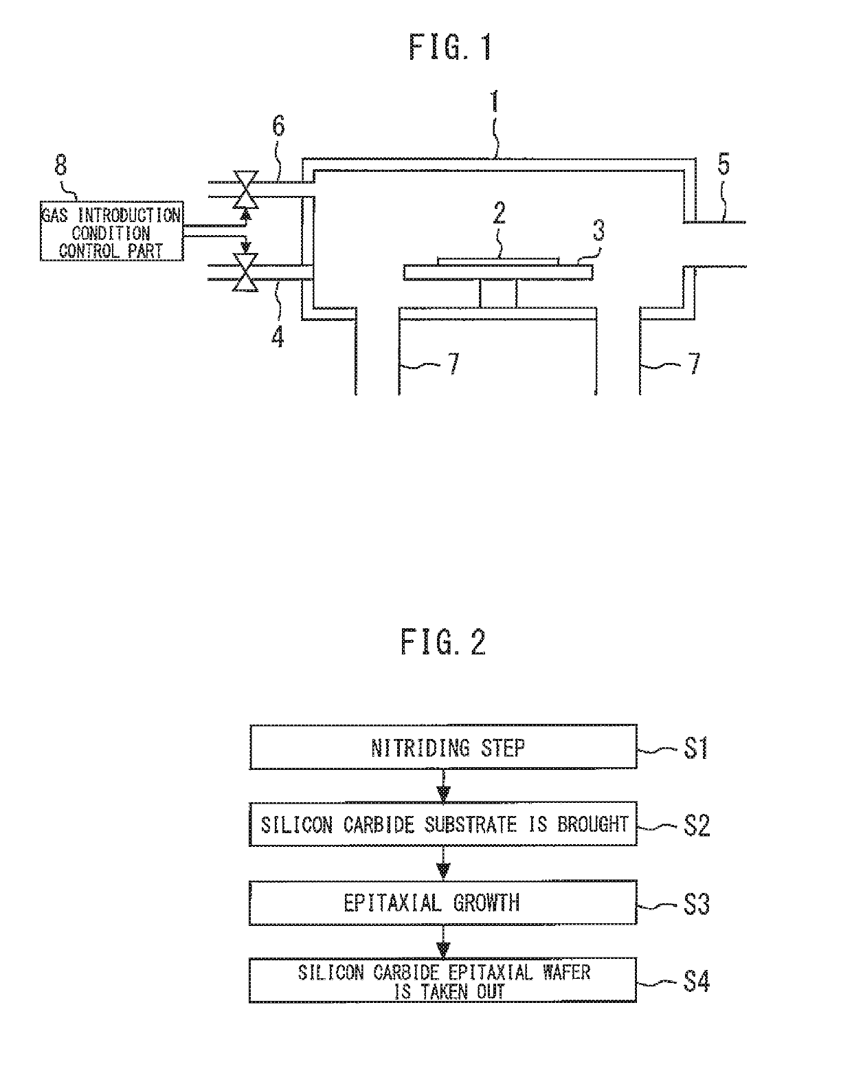
[0020]FIG. 1 is a sectional view of an apparatus for manufacturing a silicon carbide epitaxial wafer according to a first embodiment of the present invention. A wafer holder 3 on which a silicon carbide substrate 2 is mounted is provided in a growth furnace 1 for performing epitaxial growth. A first gas introduction port 4 leads a carrier gas and a raw material gas into the growth furnace 1 as a process gas for growing a silicon carbide epitaxial layer. The process gas is discharged out of the growth furnace 1 through a first gas exhaust port 5.

[0021]In an epitaxial growth step, a silicon carbide epitaxial layer is formed on the silicon carbide substrate 2. Simultaneously, a silicon carbide epitaxial layer product is also attached to inner wall surfaces of the growth furnace 1, the wafer holder 3 and other members in the furnace and grows dendritically. Structurally weak thin portions of the product in dendritic form are broken and separated due to fluctuations of gas flows at the t...

second embodiment

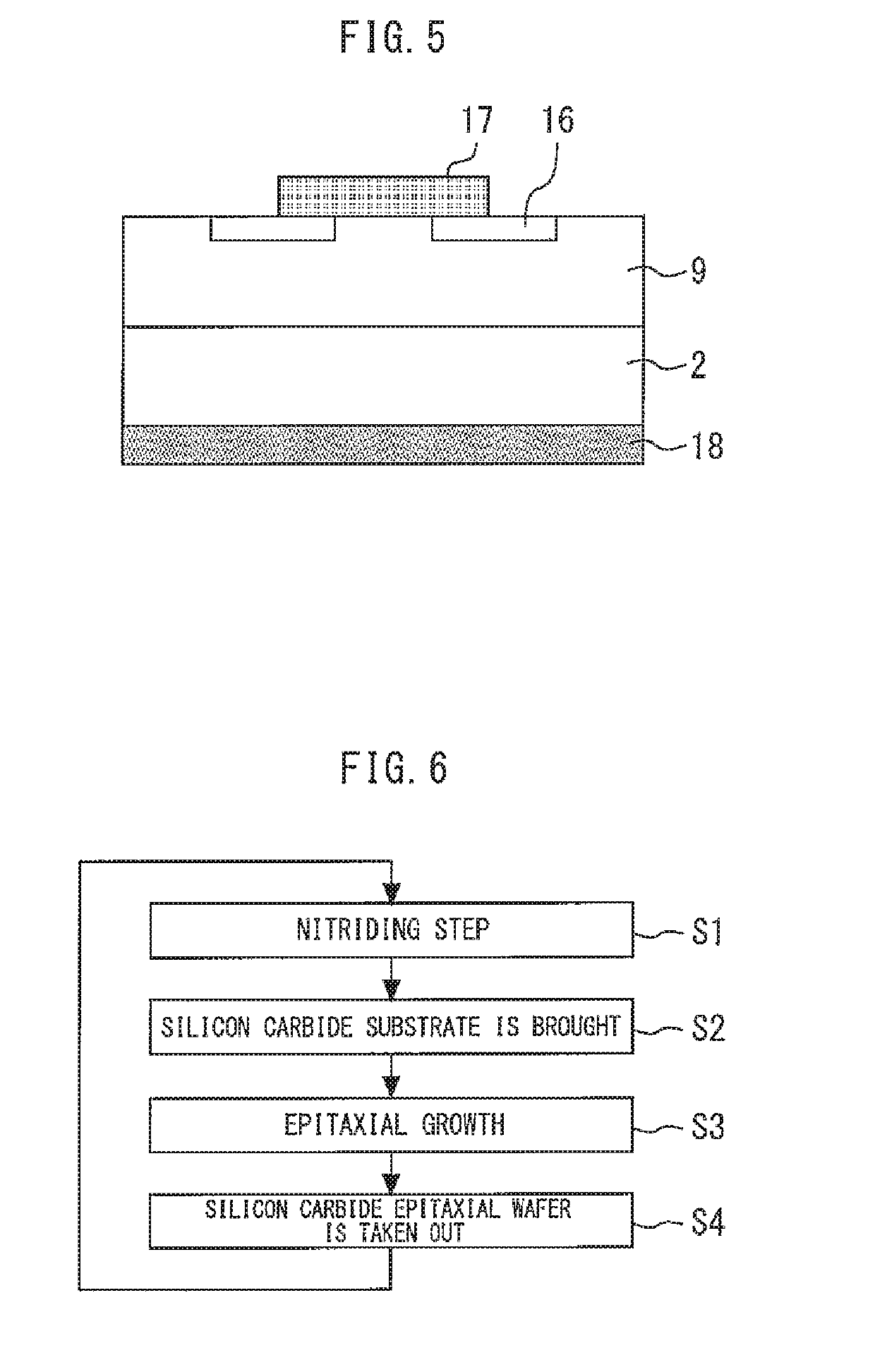
[0039]FIG. 6 is a flowchart showing a method of manufacturing a silicon carbide epitaxial wafer according to a second embodiment of the present invention. A manufacturing apparatus used in the second embodiment is the same as that in the first embodiment.

[0040]First, steps S1 to S4 are performed, as in the first embodiment. Next, the silicon carbide epitaxial wafer is taken out of the growth furnace 1 and steps S1 to S4 are thereafter repeated, thereby manufacturing a plurality of silicon carbide epitaxial wafers. By alternately repeating the nitriding step and epitaxial growth as described above, the state of bonding of silicon carbide attached to the inner wall surfaces of the growth furnace 1 and the wafer holder 3 can be stabilized at all times. As a result, the deposited film is stabilized in comparison with the case where film forming processing is successively performed a number of times after the nitriding step is performed one time, and a large amount of silicon carbide epi...

third embodiment

[0041]FIG. 7 is a growth sequence showing a method of manufacturing a silicon carbide epitaxial wafer according to a third embodiment of the present invention. Also in the third embodiment, a step similar to the same processing as that in step S3 in the first embodiment is performed, that is, the growth furnace 1 is heated to about 1650° C. and the raw-material gas is thereafter supplied into the growth furnace 1 from the first gas introduction port 4, thereby epitaxially growing a silicon carbide film having a film thickness of 10 μm on the silicon carbide substrate 2. For example, silane gas (SiH4) is supplied at a flow rate of 500 sccm as a Si atom supply source, and propane gas (C3H8) is supplied at a flow rate of 200 sccm as a C atom supply source. Nitrogen gas is used for N-type doping. Nitrogen gas is supplied for N-type doping so that the carrier concentration is 1×10¹⁷ / cm3 at the substrate interface and is 8×10¹⁵ / cm3 in the active region. Thereafter, supply of the raw-mater...


PUM

PropertyMeasurementUnit
temperatureaaaaaaaaaa
thicknessaaaaaaaaaa

Abstract

A silicon carbide epitaxial wafer manufacturing method includes: a stabilization step of nitriding, oxidizing or oxynitriding and stabilizing silicon carbide attached to an inner wall surface of a growth furnace; after the stabilization step, a bringing step of bringing a substrate in the growth furnace; and after the bringing step, a growth step of epitaxially growing a silicon carbide epitaxial layer on the substrate by supplying a process gas into the growth furnace to manufacture a silicon carbide epitaxial wafer.

Description

BACKGROUND OF THE INVENTIONField[0001]The present invention relates to a silicon carbide epitaxial wafer manufacturing method, a silicon carbide semiconductor device manufacturing method and a silicon carbide epitaxial wafer manufacturing apparatus.Background[0002]In recent years, silicon carbide (SiC) semiconductors whose bandgap, dielectric breakdown electric field intensity, saturated drift velocity and thermal conductivity are each higher than the corresponding value of silicon semiconductors have attracted attention mainly as a material for power devices for power control. In fact, power devices using such SiC semiconductors can have a markedly reduced power loss, can be made smaller in size, enable energy saving at the time of power conversion for power supply, and are, therefore, key devices in realizing a low-carbon society, for example, by improving the performance of electric vehicles and by improving the functions of solar battery systems and the like. Examples of such po...

Claims


Application Information

Patent Timeline
Patent Type & Authority Patents(United States)
IPC IPC(8): C30B29/36C30B25/20C30B25/14C23C16/32H01L21/02
CPCC30B29/36C23C16/325C30B25/14H01L21/02658H01L21/0262H01L21/02378H01L21/02529C30B25/20H01L21/67011H01L21/02167H01L21/02293H01L21/205H01L21/324
Inventor OHNO, AKIHITOHAMANO, KENICHIKANAZAWA, TAKASHI
Owner MITSUBISHI ELECTRIC CORP
Why Eureka
Try Eureka