Flash memory controller

a flash memory controller and controller technology, applied in the field of flash memory controllers, can solve the problems of occupying the flash memory interface and not being able to transfer competing data, and achieve the effect of eliminating skews and improving io throughpu

Inactive Publication Date: 2015-03-31
INT BUSINESS MASCH CORP
View PDF12 Cites 0 Cited by
  • Summary
  • Abstract
  • Description
  • Claims
  • Application Information

AI Technical Summary

Benefits of technology

[0008]A Flash memory controller according to an embodiment of the present invention may be coupled to a first Flash memory package through a first Flash memory interface. A second Flash memory package may also be coupled to the Flash memory controller through the first Flash memory interface. The Flash memory controller is designed to receive a first instruction relating to the first Flash memory package and to perform a first process depending on the first instruction. The Flash memory controller is further designed to receive a second instruction relating to the second Flash memory package and to perform a second process depending on a second instruction. The Flash memory controller is further designed for splitting the first process into at least two first sub-steps and for splitting the second process into at least two second sub-steps. The Flash memory controller is further designed for executing the first and second sub-steps and for interleaving execution of first and second sub-steps. This Flash memory controller may improve IO throughput on the Flash memory interface and may eliminates a skew between the times required for executing read and write instruction.
[0010]The Flash memory controller may further maintain a timer for an unfinished process, wherein the timer is adapted for triggering an event upon completion of a sub-step of the unfinished process. This may allow to efficiently pipeline sub-steps of multiple processes.
[0015]The first Flash memory package may comprise a first chip die. The first instruction may then relate to the first chip die of the first Flash memory package. The Flash memory controller may then be designed to receive a third instruction relating to the first chip die of the first Flash memory package and to perform a third process depending on the third instruction. The Flash memory controller is then designed for splitting the third process into at least two third sub-steps and for finishing execution of all first sub-steps before starting execution of a third sub-step. This may assure that two processes involving the same die are not executed in parallel. This may avoid an eventual corruption of data.
[0018]The Flash memory controller may comprise a flag that marks the first Flash memory interface as busy or as free. This may allow for keeping track whether the first Flash memory interface is currently available or occupied.
[0020]A method for operating a Flash memory controller according to an embodiment of the present invention comprises steps in which the Flash memory controller receives a first instruction relating to a first Flash memory package coupled to the Flash memory controller through a first Flash memory interface, in which the Flash memory controller receives a second instruction relating to a second Flash memory package coupled to the Flash memory controller through the first Flash memory interface, in which the Flash memory controller splits a first process depending on the first instruction into at least two first sub-steps, in which the Flash memory controller splits a second process depending on the second instruction into at least two second sub-steps, and in which the Flash memory controller executes the first and second sub-steps, wherein the Flash memory controller interleaves execution of first and second sub-steps. This method may improve IO throughput on the Flash memory interface and may eliminate a skew between the times required for executing read and write instructions.
[0023]This may allow for pipelining sub-steps of several completing processes, thereby reducing the overall execution time of all processes.

Problems solved by technology

During the transfer of the data from the Flash memory package to the Flash memory controller, the Flash memory interface is occupied and not available for competing data transfers.

Method used


Image

  • Flash memory controller
  • Flash memory controller
  • Flash memory controller

Examples


Embodiment Construction

Brief Description of the Drawings

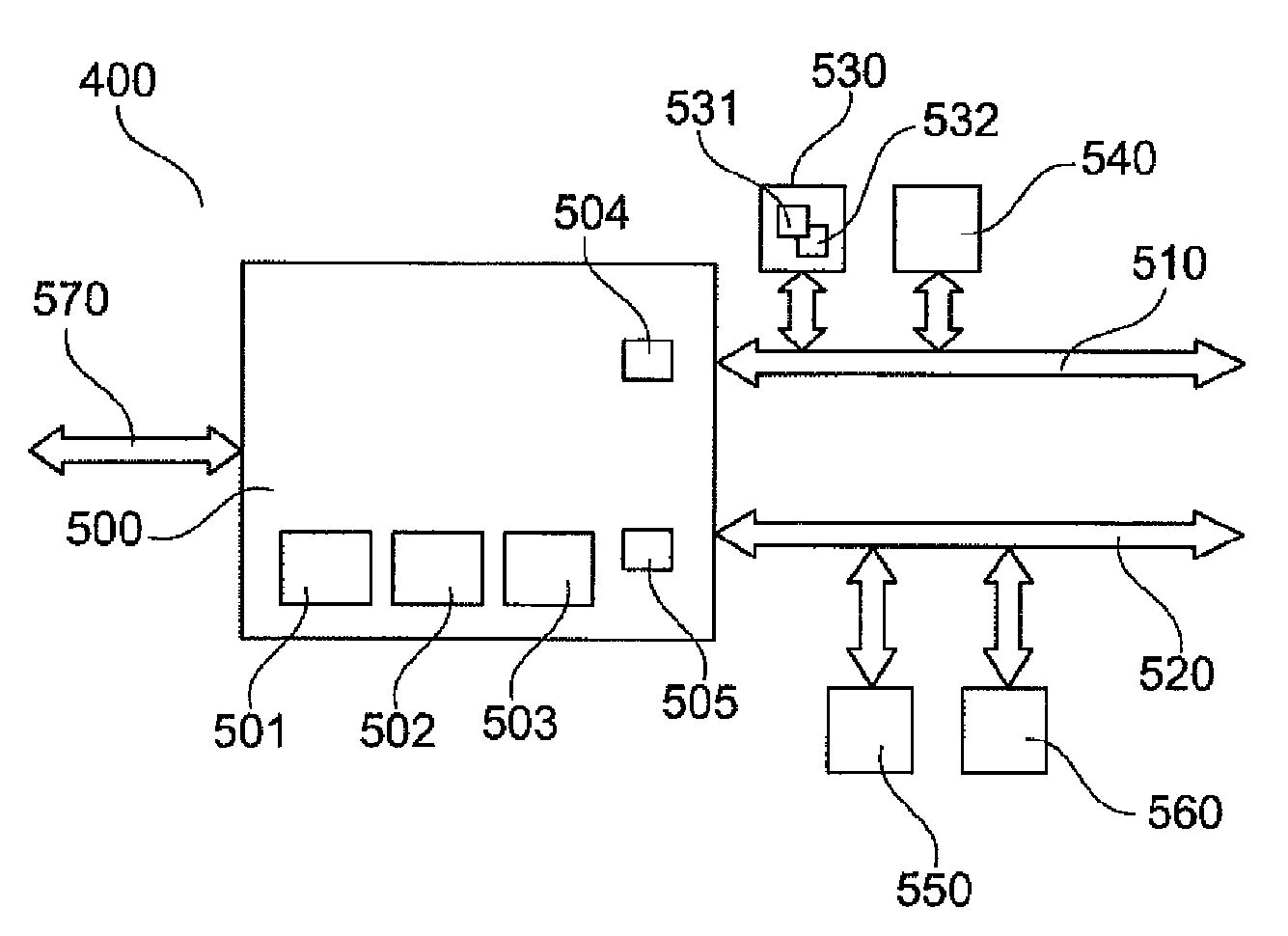
[0025]FIG. 1 depicts a schematic representation of a Flash memory system with a Flash memory controller;

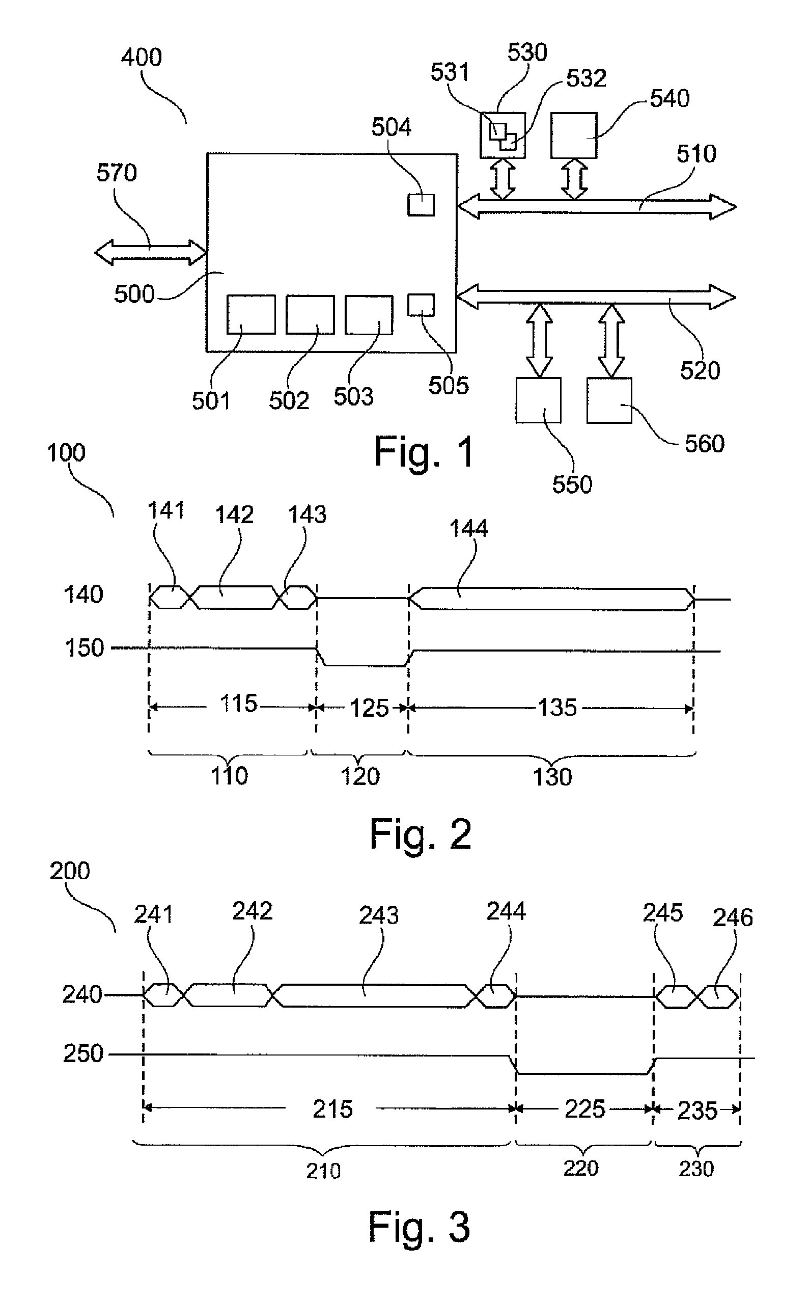
[0026]FIG. 2 shows a timing diagram of a read process;

[0027]FIG. 3 shows a timing diagram of a write process;

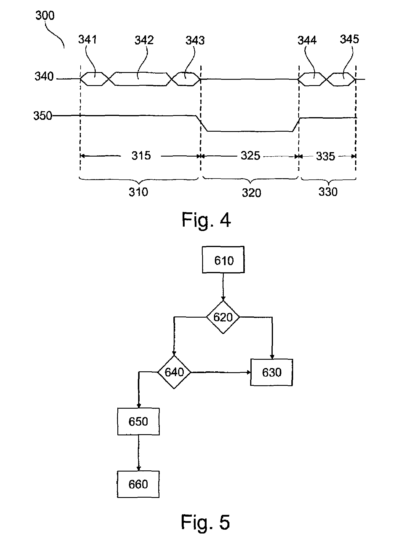
[0028]FIG. 4 shows a timing diagram of an erase process;

[0029]FIG. 5 shows a schematic flow diagram of a method for operating a Flash memory controller; and

[0030]FIG. 6 shows a schematic flow diagram of further steps of a method for operating a Flash memory controller.

[0031]FIG. 1 shows a simplified schematic representation of a Flash memory system 400. The Flash memory system 400 may for example be a Flash storage device and may for example serve as a replacement for a hard disc drive. The Flash memory system 400 may also be a portable storage device. The Flash memory system 400 comprises a Flash memory controller 500. The Flash memory controller 500 comprises a host interface 570 through which the Flash memory controller 500 may communicat...


PUM


Abstract

A Flash memory controller is coupled to a first Flash memory package through a first Flash memory interface and to a second Flash memory package through the first Flash memory interface. The Flash memory controller is designed to receive a first instruction relating to the first Flash memory package and to perform a first process depending on the first instruction. The Flash memory controller is further designed to receive a second instruction relating to the second Flash memory package and to perform a second process depending on the second instruction. The Flash memory controller is further adapted for splitting the first process into at least two first sub-steps and for splitting the second process into at least two second sub-steps. The Flash memory controller is further adapted for executing the first and second sub-steps, and for interleaving execution of first and second sub-steps.

Description

CROSS-REFERENCE TO RELATED APPLICATIONS[0001]The present invention relates to and claims the benefit of the filing date of commonly-owned, co-pending PCT Patent Application No. PCT / IB2010 / 055684, filed Dec. 9, 2010, which further claims the benefit of priority date of commonly-owned, co-pending European Patent Application No. EP 09178949.5, filed on Dec. 11, 2009, the entire contents and disclosure of which is incorporated by reference as if fully set forth herein.TECHNICAL FIELD[0002]The present invention relates to a Flash memory controller and to a method for operating a Flash memory controller.BACKGROUND OF THE INVENTION[0003]Solid-state based storage devices are becoming increasingly popular due to their low power consumption, ruggedness and high input-output (IO) performance compared to conventional hard disc drives. Most current solid-state storage devices are based on NAND-flash memory chips.[0004]A typical configuration of a Flash-based storage system comprises at least one...

Claims


Application Information

Patent Timeline
Patent Type & Authority Patents(United States)
IPC IPC(8): G06F12/02G06F9/30G06F13/16G11C7/10
CPCG06F13/1668G11C7/1042G06F9/3004
Inventor ELEFTHERIOU, EVANGELOS S.HAAS, ROBERTHU, XIAO-YU
Owner INT BUSINESS MASCH CORP
Why Eureka
Try Eureka