Method for solventless quantum dot exchange

a quantum dot exchange and solvent technology, applied in the direction of non-metal conductors, conductors, sustainable buildings, etc., can solve the problems of poor color rendering, poor power efficiency, and number of critical shortfalls

Active Publication Date: 2015-04-14
SHOEI CHEM IND CO LTD
View PDF158 Cites 71 Cited by
  • Summary
  • Abstract
  • Description
  • Claims
  • Application Information

AI Technical Summary

Problems solved by technology

Unfortunately, existing rare-earth activated phosphors or halophosphates, which are currently the primary source for solid-state down-conversion, were originally developed for use in fluorescent lamps and cathode ray tubes (CRTs), and therefore have a number of critical shortfalls when it comes to the unique requirements of SSWL.
As such, while some SSWL systems are available, poor power efficiency ($200 / kilolumen (klm)) limit this technology to niche markets such as flashlights and walkway lighting.
Furthermore, LEDs often suffer from reduced performance as a result of internal reflection of photons at the chip / coating interface.
Currently these coatings are made by using an inorganic or organic coating that has a very different refractive index than the base material (i.e., the chip), which results in a detrimental optical effect due to the refractive index mismatch at the interface between the two materials.
The resulting LED structure suffers loss of light at the chip / compliant polymer interface due to the lower refractive index of the polymer coating in relation to the LED.
However, if the refractive index of the compliant layer is increased, even greater loss will occur due at the high refractive index / low refractive index interface between the compliant polymer and the hard shell polymer due to internal reflection.
There are several critical factors which result in poor power efficiencies when using traditional inorganic phosphors for SSWL.
These include: total internal reflection at the LED-chip and phosphor layer interface resulting in poor light extraction from the LED into the phosphor layer; poor extraction efficiency from the phosphor layer into the surroundings due to scattering of the light generated by the phosphor particles as well as parasitic absorption by the LED chip, metal contacts and housing; broad phosphor emission in the red wavelength range resulting in unused photons emitted into the near-IR; and poor down-conversion efficiency of the phosphors themselves when excited in the blue wavelength range (this is a combination of absorption and emission efficiency).
While efficiencies improve with UV excitation, additional loss due to larger Stokes-shifted emission and lower efficiencies of LEDs in the UV versus the blue wavelength range makes this a less appealing solution overall.
As a result, poor efficiency drives a high effective ownership cost.
The cost is also significantly impacted from the laborious manufacturing and assembly process to construct such devices, for example the heterogeneous integration of the phosphor-layer onto the LED-chip during packaging (DOE and Optoelectronics Industry Development Association “Light emitting diodes (LEDs) for general illumination,” Technology Roadmap (2002)).
However, many of the current filters allow photon emission from the blue end of the spectrum, thus limiting the quality of the white LED.
The performance of the devices also suffer from poor color rendering due to a limited number of available phosphor colors and color combinations that can be simultaneously excited in the blue.
While some development of organic phosphors has been made for SSWL, organic materials have several insurmountable drawbacks that make them unlikely to be a viable solution for high-efficiency SSWL.
These include: rapid photodegradation leading to poor lifetime, especially in the presence of blue and near-UV light; low absorption efficiency; optical scattering, poor refractive index matching at the chip-interface, narrow and non-overlapping absorption spectra for different color phosphors making it difficult or impossible to simultaneously excite multiple colors; and broad emission spectra.

Method used


Image

  • Method for solventless quantum dot exchange
  • Method for solventless quantum dot exchange
  • Method for solventless quantum dot exchange

Examples


example 1

GP-988 and Green Nanocrystal Paste

[0073]After the shell synthesis, the toluene nanocrystal solution is washed in 2× volume of ethanol, where the nanocystals precipitate, and settle into a compact cake using a centrifuge. The wash solvent is then decanted off of the wet cake, and the pasty cake is then used in the exchange. For QD synthesis and shelling references, See Alivisatos, A. P., “Semiconductor clusters, nanocrystals, and quantum dots,” Science 271:933 (1996); X. Peng, M. Schlamp, A. Kadavanich, A. P. Alivisatos, “Epitaxial growth of highly luminescent CdSe / CdS Core / Shell nanocrystals with photostability and electronic accessibility,” J. Am. Chem. Soc. 30:7019-7029 (1997); and C. B. Murray, D. J. Norris, M. G. Bawendi, “Synthesis and characterization of nearly monodisperse CdE (E=sulfur, selenium, tellurium) semiconductor nanocrystallites,” J. Am. Chem. Soc. 115:8706 (1993), X. Peng, et al., J. Am. Chem. Soc. 30:7019-7029 (1997).

[0074]1.5 g GP-988 was added to green nanocryst...

example 2

GP-988 and Red Nanocrystal Paste

[0077]2.25 g GP-988 was added to red nanocrystal paste (from 15 mL washed nanocrystal, which was decanted of its wash solvent), stirred well with a spatula, and then a stir bar while heating to 90° C. for 2 hours. The solution was cooled to room temperature and decanted to another vial.

example 3

Preparation of Nanocrystal Film

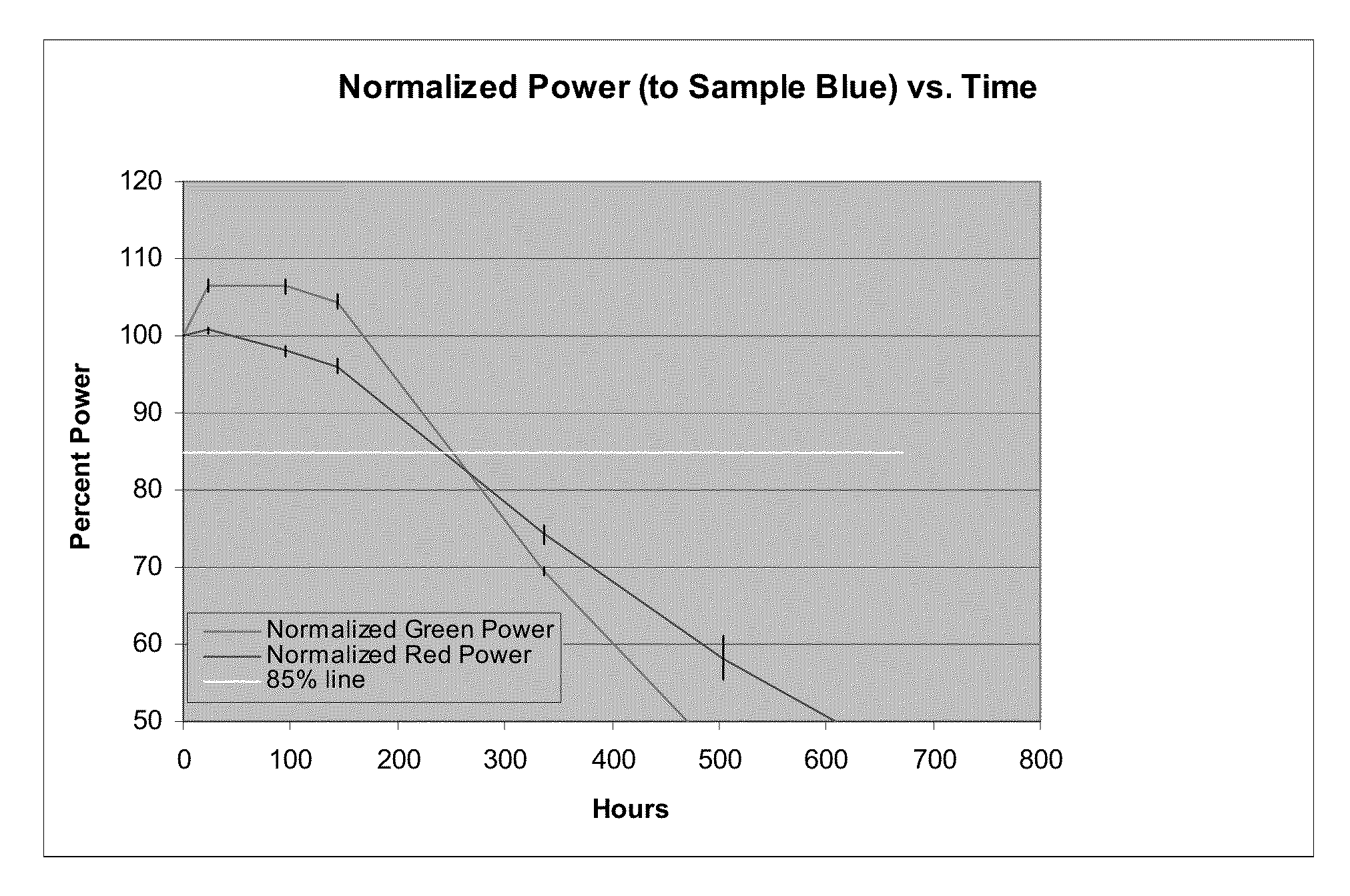
[0078]A film was made from green concentrate in Example 1 and red concentrate in Example 2 in Epic 91 epoxy. The accelerated reliability test shows similar stability to POR ESH films, specifically, 275 hr lifetime on an accelerated testing platform (lightbox III) which is in the range of standard solvent processed material films


PUM

PropertyMeasurementUnit
Tgaaaaaaaaaa
Tgaaaaaaaaaa
Tgaaaaaaaaaa

Abstract

The present invention describes a solventless ligand exchange using a siloxane polymer having a binding ligand that displaces the binding ligand on a quantum dot material.

Description

CROSS-REFERENCES TO RELATED APPLICATIONS[0001]This application claims priority to U.S. Provisional Application No. 61 / 781,285, filed Mar. 14, 2013, which is incorporated in its entirety herein for all purposes.BACKGROUND OF THE INVENTION[0002]High performance down-converting phosphor technologies will play a prominent role in the next generation of visible light emission, including high efficiency solid-state white lighting (SSWL). In addition, such technologies are also applicable to near infrared (NIR) and infrared (IR) light emitting technologies. Down-conversion from ultraviolet (UV) or blue light emitting semiconductor light emitting diodes (LEDs) into blue, red and green wavelengths offers a fast, efficient and cost-effective path for delivering commercially attractive white light sources. Unfortunately, existing rare-earth activated phosphors or halophosphates, which are currently the primary source for solid-state down-conversion, were originally developed for use in fluores...

Claims


Application Information

Patent Timeline
Patent Type & Authority Patents(United States)
IPC IPC(8): C09K11/54C09K11/02
CPCC09K11/02Y10S977/773Y10S977/774C09K11/025C09K11/08Y02B20/00
Inventor FURUTA, PAUL T.DUBROW, ROBERT
Owner SHOEI CHEM IND CO LTD
Why Eureka
Try Eureka