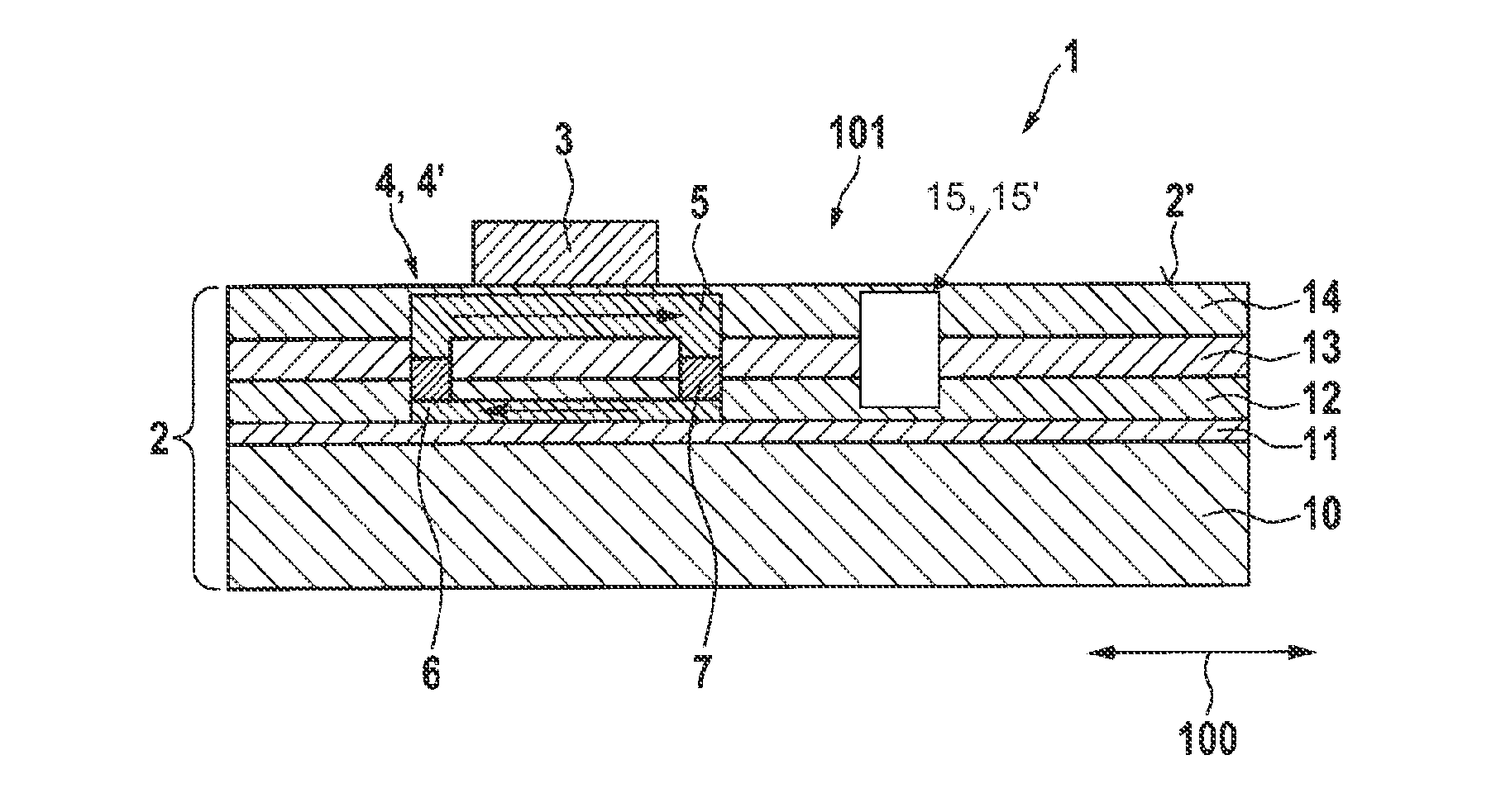
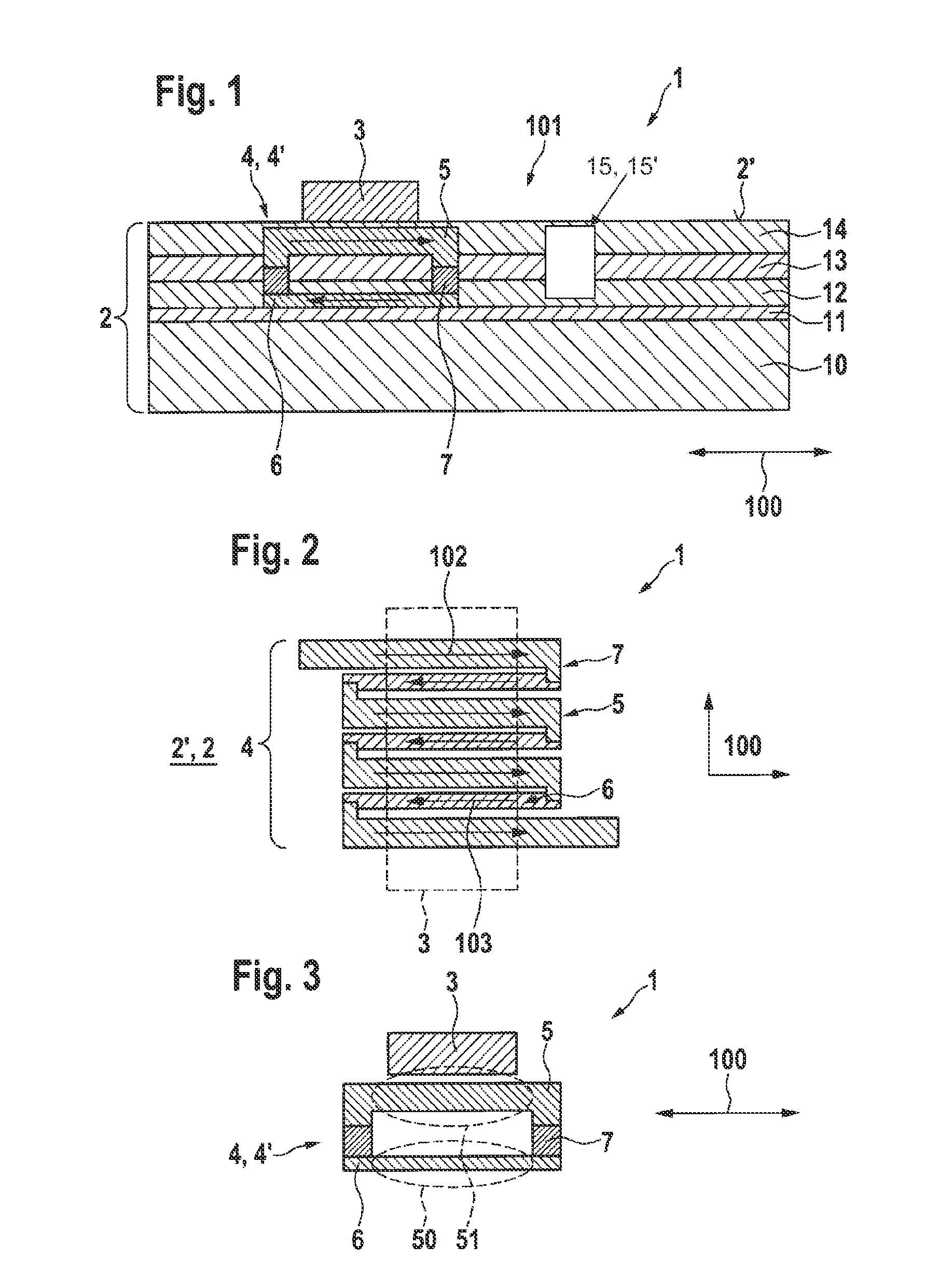
[0004]An example magnetic field sensor, according to the present invention, and example method according to the present invention, for producing a magnetic field sensor, may have the advantage that a comparatively compact installation space is made possible, and consequently a cost-effective implementation of a magnetic field sensor, at the same time, contamination in the production of the magnetic field sensor by foreign materials being excluded, especially during the insertion of the magnetic core. The example magnetic field sensor according to the present invention is thereby advantageously producible in a standard semiconductor production process, especially in a CMOS process. This is achieved in that the excitation coil has a coil cross section which is aligned essentially perpendicular to the main plane of extension of the substrate, the magnetic core being preferably situated on the substrate in the radial direction of the coil cross section outside the coil cross section. This has the advantage that the production of electrical and electronic structures in the substrate, and particularly the production of excitation coils and / or detection coils in the substrate take place independently of the situation of the magnetic core on the substrate, and consequently, is able to be implemented in standard semiconductor production methods, particularly in a CMOS process. The introduction of foreign particles in the substrate is excluded, in this context. The magnetic core, in particular, is situated on a surface of the substrate only after the sealing of the substrate. The concept “coil cross section”, within the meaning of the present invention, includes especially that surface of the excitation coil which is aligned perpendicular to the magnetic field induced by the excitation coil and is bordered on the outside by the windings of the excitation coil. In an advantageous manner, in spite of the situation of the magnetic core outside the excitation coil, a magnetic flux is induced in the magnetic core by the excitation coil, which is available for sensor situation according to the “fluxgate” sensor principle. In any desired specific embodiment, the substrate preferably includes a semiconductor substrate and, especially preferred, a silicon substrate.
[0005]According to one preferred specific embodiment, it is provided that the magnetic core is situated perpendicular to the main plane of extension, outside the coil cross section and preferably on an, in particular, outer surface of the substrate. Consequently, in an advantageous manner, a comparatively simple and cost-saving production of the magnetic field sensor is made possible by situating the magnetic core simply on or perpendicular to the main plane of extension above the excitation coil, after the production of the electrical and electronic structures in the substrate, particularly in a standard CMOS process. This is preferably carried out in a self-contained production process. A surface, within the meaning of the present invention, includes particularly a planar surface of the substrate and / or an indentation on a surface of the substrate, into which the magnetic core is inserted.
[0006]According to one preferred specific embodiment it is provided that the substrate includes a layer construction, the excitation coil including a plurality of supply conductors and a plurality of return conductors; the plurality of supply conductors and the plurality of return conductors being preferably situated in different layers of the layer construction, perpendicular to the main plane of extension and / or on different sides of the substrate. Consequently, it is particularly advantageous that the excitation coil is producible in standard semiconductor production methods, the supply conductors and the return conductors being implemented in different metallization planes, which are preferably connected to one another using electrical contact elements, so-called “vias”. This makes possible a comparatively cost-effective production of a magnetic field sensor. The return conductors are used particularly to connect the individual supply conductors of the plurality of supply conductors to one another in an electrically conductive manner. The plurality of supply conductors are situated particularly preferably on the back side of the substrate. Consequently, in an advantageous manner, the distance between supply conductors and return conductors is comparatively large, so that a greater electrical field is achieved.
[0008]According to one preferred specific embodiment, it is provided that, perpendicular to the main plane of extension, the plurality of supply conductors is situated generally between the magnetic core and the plurality of return conductors. Consequently, in an advantageous manner, the distance between the magnetic core and the supply conductors is clearly less than the distance between the magnetic core and the return conductors, so that the magnetic flux, which is generated by the supply conductors at the location of the magnetic core, is clearly greater than the magnetic flux that is generated by the return conductors in the area of the magnetic core. The resulting total magnetic flux is thus determined by the magnetic flux generated by the supply conductors, and is not equal to zero, so that the magnetic core is brought to magnetic saturation by a current flow in the excitation coil. The magnetic core preferably includes a soft magnetic material and particularly an iron-nickel alloy. Thus, the magnetic core is comparatively easy to magnetize.
[0011]The present invention further provides an example method for producing a magnetic field sensor, the substrate being provided in a first production step; the excitation coil being produced in the substrate in a second production step; and in a third production step, the magnetic core being positioned in the radial direction of the coil cross section, outside the coil cross section. Thus, a clearly more cost-effective production of a comparatively compact installation space magnetic field sensor is made possible. This is achieved in that the first and the second production step in standard semiconductor production processes, especially in a standard CMOS process, are able to be implemented, so that only in the third production step an additional method is required, in which only the magnetic core has to be positioned on the substrate in the area of the excitation coil. In particular, positioning the magnetic core during the production of the excitation coil is not necessary, so that contamination of the semiconductor material, by magnetic core materials, is prevented. In an advantageous manner, in spite of the situation of the magnetic core outside the excitation coil, a magnetic flux is induced in the magnetic core by the excitation coil, which is available for sensor situation according to the “fluxgate” sensor principle.
[0012]According to one preferred specific embodiment, it is provided that, in the third production step, the magnetic core is positioned perpendicular to the main plane of extension, outside the coil cross section, and preferably on a, particularly, outer surface of the substrate, so that the third production step is able to be carried out comparatively simply and cost-effectively.

