Microstructure manufacturing method

a manufacturing method and microstructure technology, applied in the direction of liquid/solution decomposition chemical coating, instruments, imaging devices, etc., can solve the problems of difficult to obtain a desirable phase image, difficult to obtain an image of soft material or soft tissue using these techniques, and more places of sticking of periodic structur

Inactive Publication Date: 2015-05-26
CANON KK
View PDF4 Cites 1 Cited by
  • Summary
  • Abstract
  • Description
  • Claims
  • Application Information

AI Technical Summary

Benefits of technology

[0008]Aspects of the present invention are directed to a microstructure manufacturing method enabling manufacturing of a metal microstructure having little shifts of the pitch.

Problems solved by technology

However, it is difficult to obtain an image of a soft material or a soft tissue using these techniques because the soft material or the soft tissue absorbs only a little X-ray.
But, as a pitch of the periodic structure becomes narrower and an aspect ratio of the periodic structure becomes higher, sticking of the periodic structure occurs in more places.
So, it is difficult to obtain a desirable phase image when the X-ray Talbot interferometer uses the absorption grating having many shifts of the pitch.

Method used


Image

  • Microstructure manufacturing method
  • Microstructure manufacturing method
  • Microstructure manufacturing method

Examples


first example

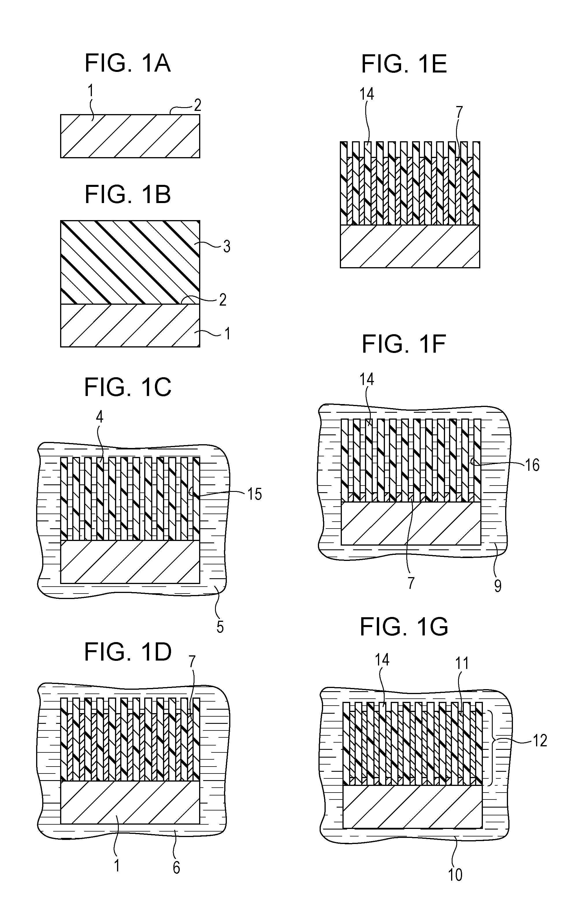
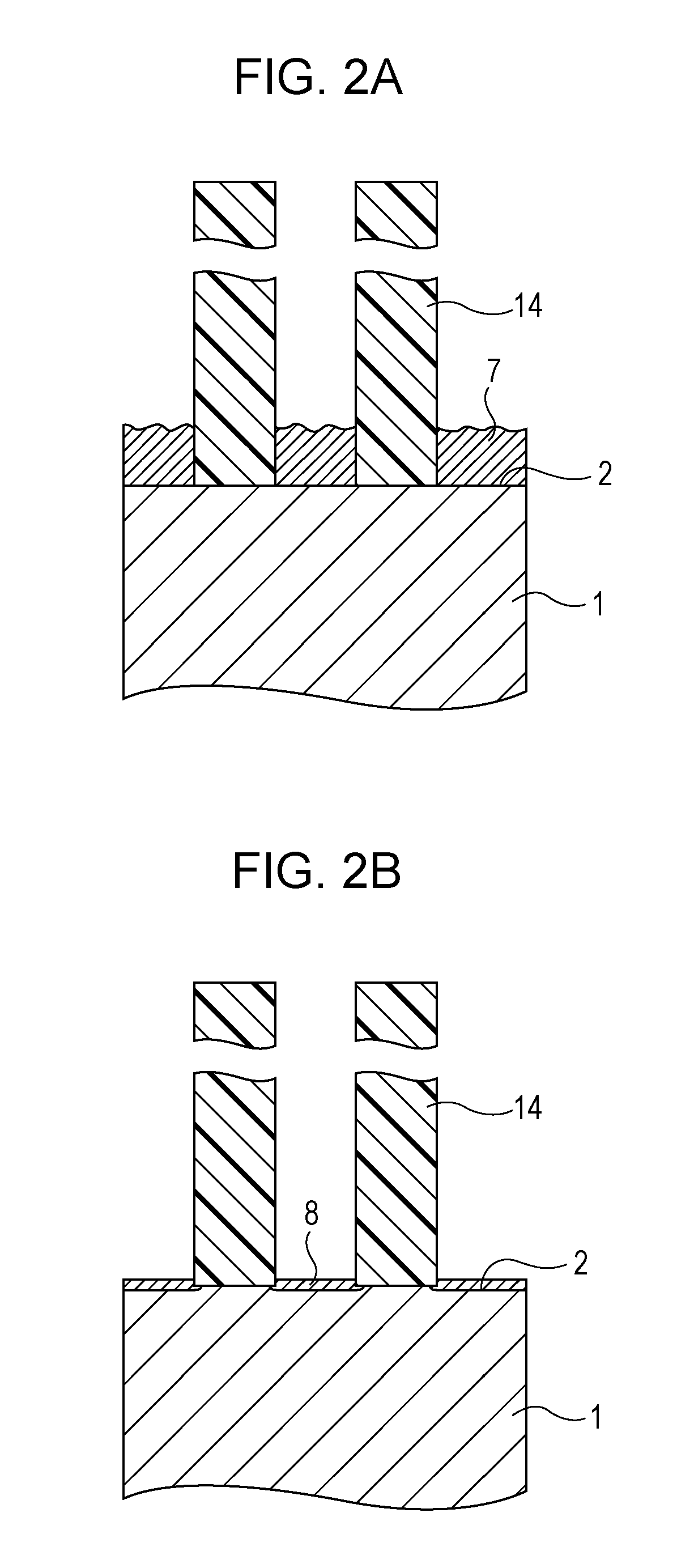
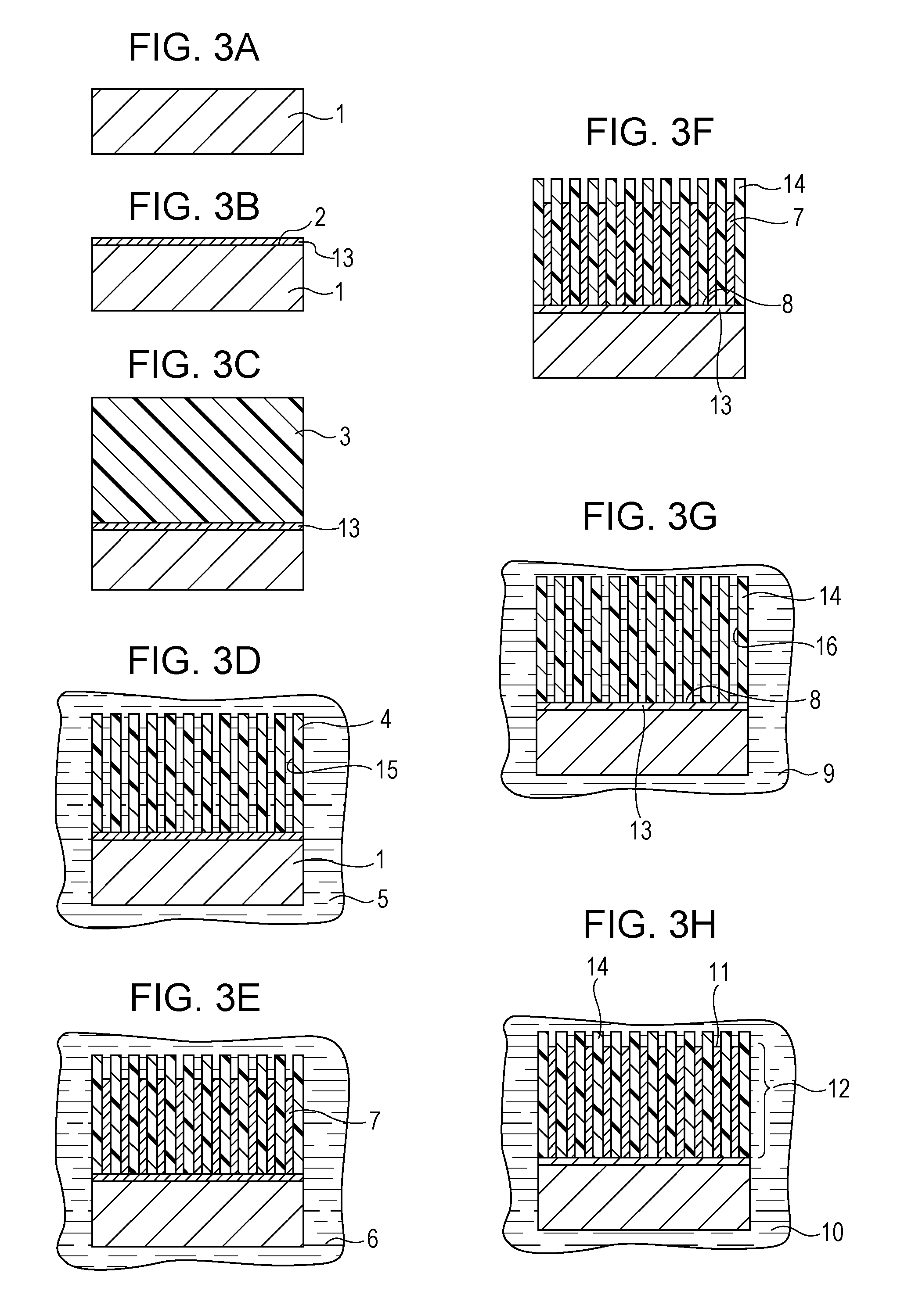
[0050]FIGS. 3A to 3h illustrate a first example according to the microstructure manufacturing method of the present invention.

[0051]In the present example, a silicon wafer is used as the substrate 1 (FIG. 3A). The wafer is double sided, and its diameter is 4 inches and its thickness is 525 μm. A titanium film with a thickness of 5 nm and a gold film with a thickness of 100 nm are formed sequentially in this order on the substrate 1 as the electrically conductive layer 13 by an electron beam deposition apparatus (FIG. 3B).

[0052]The negative resist of SU-8 (manufactured by KAYAKU Micro Chemical Co., Ltd) is used as the photosensitive resin. The SU-8 is applied on the electrically conductive layer 13, and a photosensitive resin layer 3 with a thickness of 40 μm is formed, the photosensitive resin layer 3 is soft-baked at 95° C. for ten minutes (FIG. 3C). Next, the photosensitive resin layer 3 is exposed to ultraviolet light by MPA600 (manufactured by Canon), and the exposed photosensit...

second example

[0060]FIGS. 4A to 4H illustrate a second example according to the microstructure manufacturing method of the present invention.

[0061]In the present example, a silicon wafer is used as the substrate 1 (FIG. 4A). The wafer is double sided, and its diameter is 4 inches and its thickness is 525 μm. A chromium film with a thickness of 5 nm and a platinum film with a thickness of 100 nm are formed sequentially in this order on the substrate 1 as the electrically conductive layer 13 by a vacuum sputtering apparatus (FIG. 4B).

[0062]The negative resist of SU-8 (manufactured by KAYAKU Micro Chemical Co., Ltd) is used as the photosensitive resin. The SU-8 is applied on the electrically conductive layer 13, and a photosensitive resin layer 3 with a thickness of 60 μm is formed, the photosensitive resin layer 3 is soft-baked at 95° C. for ten minutes (FIG. 4C). Next, the photosensitive resin layer 3 is exposed to synchrotron radiation light by X-ray exposure apparatus, and the exposed photosensi...

third example

[0068]FIGS. 5A to 5g illustrate a third example according to the microstructure manufacturing method of the present invention.

[0069]In the present example, a stainless plate is used as the substrate 1 (FIG. 5A). The substrate 1 includes the substrate surface 2 which has electrical conductivity. The negative resist of SU-8 (manufactured by KAYAKU Micro Chemical Co., Ltd) is used as the photosensitive resin. The SU-8 is applied on the stainless plate, and a photosensitive resin layer 3 with a thickness of 60 μm is formed, the photosensitive resin layer 3 is soft-baked at 95° C. for ten minutes (FIG. 5B). Next, the photosensitive resin layer 3 is exposed to synchrotron radiation light by X-ray exposure apparatus, and the exposed photosensitive resin layer 3 is baked at 65° C. for five minutes. A latent image is formed in the photosensitive resin layer 3 in such a manner that a square pole pattern 2 μm on a side is two-dimensionally arranged at the 4 μm pitch. The latent image is develo...


PUM

PropertyMeasurementUnit
aspect ratioaaaaaaaaaa

Abstract

A microstructure manufacturing method includes forming a layer of a photosensitive resin on a substrate surface having an electrical conductivity, forming a structure of the photosensitive resin by exposing the layer of the photosensitive resin to light and developing the layer of the photosensitive resin to expose a part of the substrate surface, forming a first plated layer on the exposed part of the substrate surface by soaking the structure of the photosensitive resin in a first plating solution, curing the structure of the photosensitive resin after forming the first plated layer, removing at least part of the first plated layer after curing the structure of the photosensitive resin, and forming a second plated layer on a part where the first plated layer is removed, by soaking the structure of the photosensitive resin in a second plating solution different from the first plating solution.

Description

BACKGROUND OF THE INVENTION[0001]1. Field of the Invention[0002]The present invention relates to a method for manufacturing a microstructure.[0003]2. Description of the Related Art[0004]A microstructure having a periodic structure is used in several devices as a grating. A microstructure made of gold which absorbs X-rays is used in a nondestructive inspection for industrial use or an X-ray examination for medical use. The nondestructive inspection or the X-ray examination utilizes the X-ray absorption contrast method to obtain an image of an object or a living body. However, it is difficult to obtain an image of a soft material or a soft tissue using these techniques because the soft material or the soft tissue absorbs only a little X-ray.[0005]The phase contrast method, which utilizes a phase difference of X-rays, has been studied at synchrotron radiation facilities since the 1990s. The phase contrast method using an X-ray tube instead of the synchrotron (e.g. propagation-based met...

Claims


Application Information

Patent Timeline
Patent Type & Authority Patents(United States)
IPC IPC(8): G03F1/58C25D5/12G02B5/18
CPCC25D5/12G02B5/18G03F7/40G21K1/10G21K2207/005A61B6/4233A61B6/4291A61B6/484C25D7/123C25D3/12C25D3/38C25D3/48C25D5/022C25D5/10C23C18/1605C23C18/1651C25D5/615
Inventor TESHIMA, TAKAYUKISETOMOTO, YUTAKA
Owner CANON KK
Why Eureka
Try Eureka