
Semiconductor structure for antenna switching circuit

a technology of semiconductor structure and antenna switching circuit, which is applied in the direction of semiconductor devices, electrical equipment, basic electric elements, etc., can solve the problems that the antenna switching circuit affects the signal quality and the performance of the antenna, and the voltage resistance level and anti-noise ability of the antenna switching circuit are improved, and the signal quality of the antenna is enhanced. , the effect of high marketing potential

Inactive Publication Date: 2015-05-26
MAXTEK TECH
View PDF1 Cites 0 Cited by
  • Summary
  • Abstract
  • Description
  • Claims
  • Application Information

AI Technical Summary

Benefits of technology

The invention provides a semiconductor structure and a manufacturing method for an antenna switching circuit that improves its voltage-resistant level and anti-noise ability. This is achieved by a parallel connection of an impedance to a Schottky contact formed by the hetero-interface between the gate metal and the capping layer. This results in improved signal quality and markets a high potential for the antenna.

Problems solved by technology

Accordingly, the antenna switching circuit also affects the signal quality and the performance of the antenna.

Method used


Image

  • Semiconductor structure for antenna switching circuit
  • Semiconductor structure for antenna switching circuit
  • Semiconductor structure for antenna switching circuit

Examples


Embodiment Construction

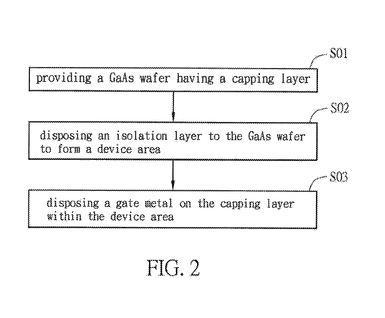
[0030]The present invention will be apparent from the following detailed description, which proceeds with reference to the accompanying drawings, wherein the same references relate to the same elements.

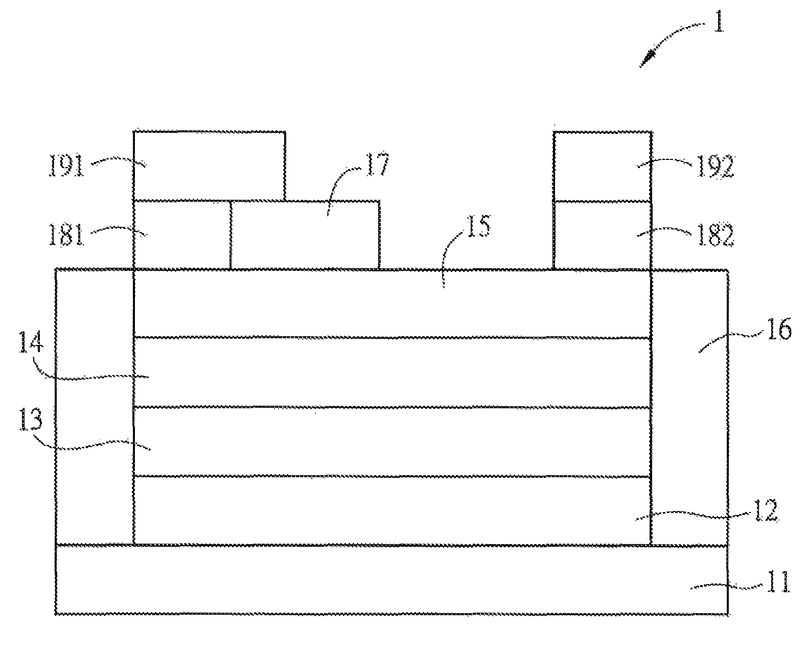
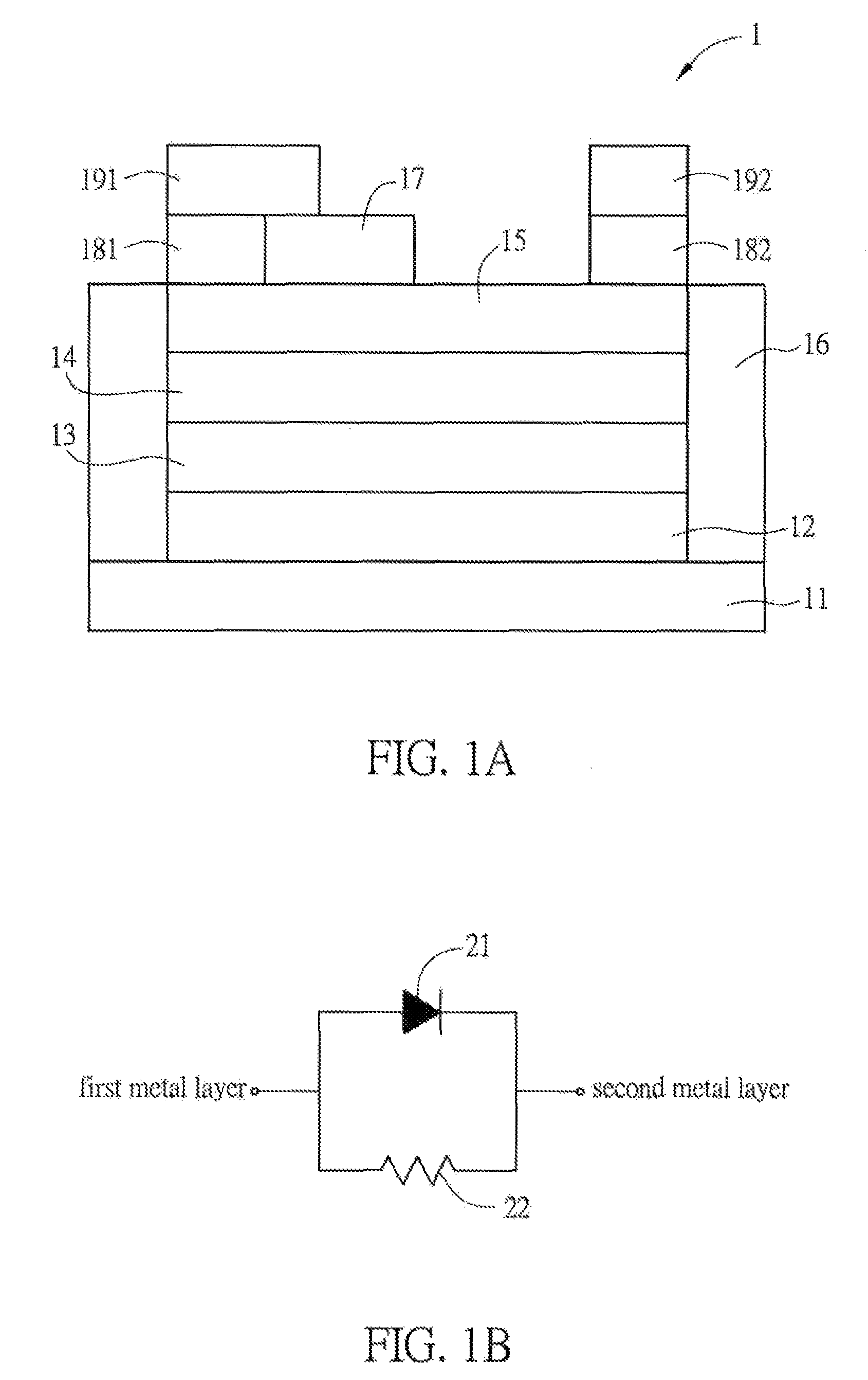
[0031]FIG. 1A is a schematic diagram of a semiconductor structure, of a preferred embodiment of the invention, for an antenna switching circuit. The semiconductor structure 1, includes a buffer layer 11, a channel layer 12, a space layer 13, a donor layer 14, a capping layer 15, an isolation layer 16 and a gate metal 17. In this embodiment, the buffer layer 11, the channel layer 12 and the space layer 13 are undoped.

[0032]The material of the buffer layer 11 is GaAs for example. Herein, the buffer layer 11 is regarded as a substrate, and other semiconductor layers can be disposed on the buffer layer 11.

[0033]The channel layer 12 is disposed on the buffer layer 11. The material of the channel layer 12 is InGaAs for example. The space layer 13 is disposed on the channel layer 12. The mat...


PUM


Abstract

A manufacturing method for antenna switching circuit includes the following steps of: providing a GaAs wafer, which includes a capping layer; disposing an isolation layer to the GaAs wafer for forming a device area; and disposing a gate metal on the capping layer within the device area, wherein an interface between the gate metal and the capping layer forms a Schottky contact, and the Schottky contact is parallel connected with an impedance. The present invention also discloses a semiconductor structure for antenna switching circuit.

Description

CROSS REFERENCE TO RELATED APPLICATIONS[0001]This Non-provisional application claims priority under 35 U.S.C. §119(a) on Patent Application No(s). 101127118 filed in Taiwan, Republic of China on Jul. 27, 2012, the entire contents of which are hereby incorporated by reference.BACKGROUND OF THE INVENTION[0002]1. Field of Invention[0003]The invention relates to a semiconductor structure and a manufacturing method thereof and, in particular, to a semiconductor structure and a manufacturing method thereof for an antenna switching circuit.[0004]2. Related Art[0005]Due to the wide development of the wireless communication technology, the marketing demand for the antenna has been raised rapidly. Nowadays, the wireless communication apparatuses, such as cell phones, notebook computers, global positioning systems, digital televisions, and portable electronic apparatuses, rely on antennas for transmitting and receiving signals. In other words, the antenna is an essential device to the wireless...

Claims


Application Information

Patent Timeline
Patent Type & Authority Patents(United States)
IPC IPC(8): H01L31/072H01L29/40H01L29/66H01L29/812H01L29/872
CPCH01L29/872H01L29/402H01L29/404H01L29/66143H01L29/812
Inventor LIAO, KE-KUNGCHANG, TUNG-SHENGKU, CHUN-YENCHEN, SHIH-YU
Owner MAXTEK TECH
Features
  • Generate Ideas
  • Intellectual Property
  • Life Sciences
  • Materials
  • Tech Scout
  • Unparalleled Data Quality
  • Higher Quality Content
  • 60% Fewer Hallucinations
Learn More