Semiconductor device and method of operating the same

a technology of semiconductor devices and circuits, applied in static storage, digital storage, instruments, etc., can solve problems such as deteriorating the reliability of 3d semiconductor devices, and achieve the effect of improving the reliability of programs

Active Publication Date: 2015-05-26
SK HYNIX INC
View PDF8 Cites 8 Cited by
  • Summary
  • Abstract
  • Description
  • Claims
  • Application Information

AI Technical Summary

Benefits of technology

[0009]Various exemplary embodiments relate to a semiconductor memory capable of improving the reliability of program, read and erase operations and a method of operating the same.

Problems solved by technology

In the 3D semiconductor device having the above configuration, threshold voltages of the memory cells, coupled adjacent to the drain selection transistor, may be changed by resistance around the source line during program and read operations, which may deteriorate the reliability of the 3D semiconductor device.

Method used


Image

  • Semiconductor device and method of operating the same
  • Semiconductor device and method of operating the same
  • Semiconductor device and method of operating the same

Examples


Embodiment Construction

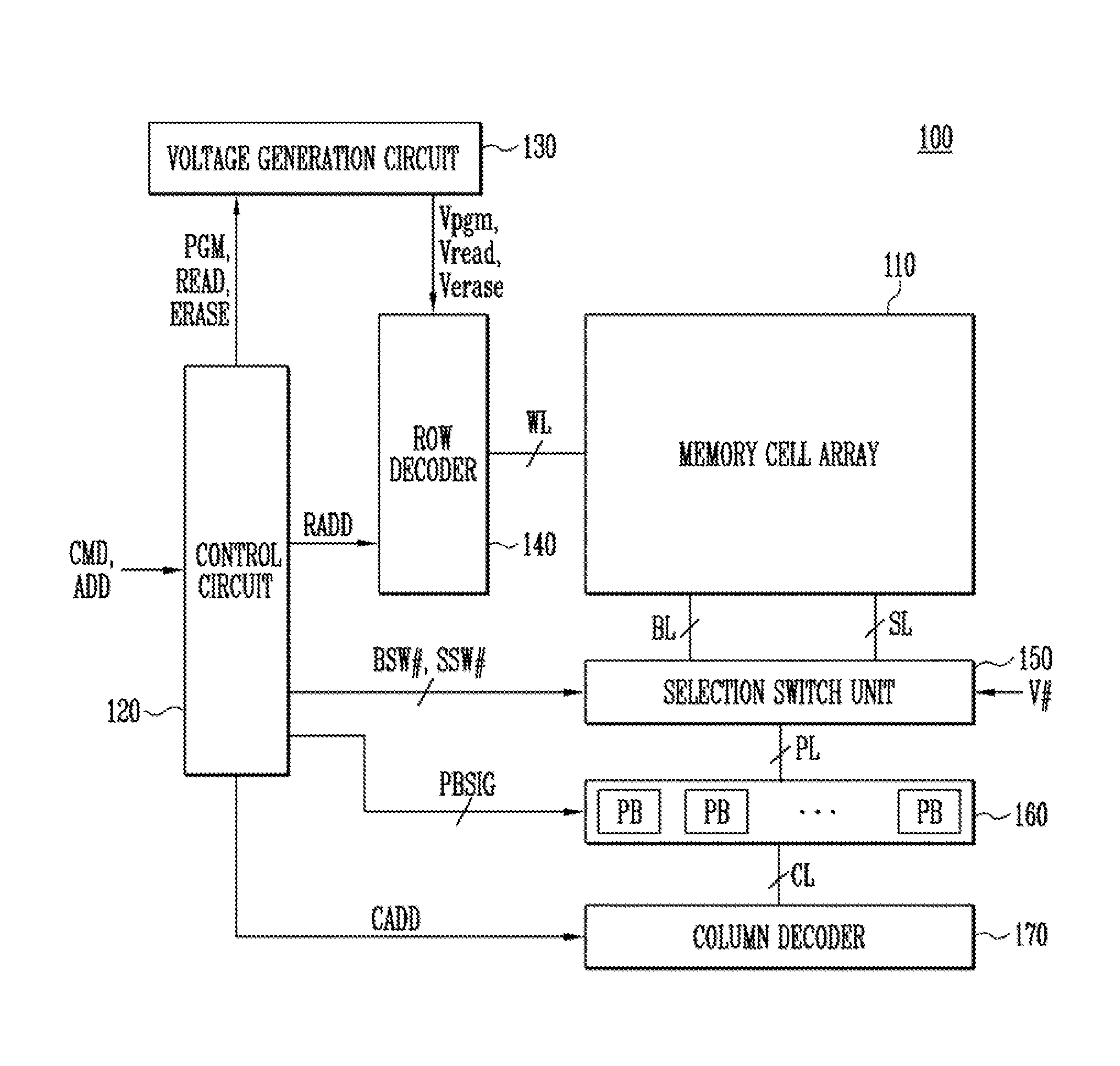
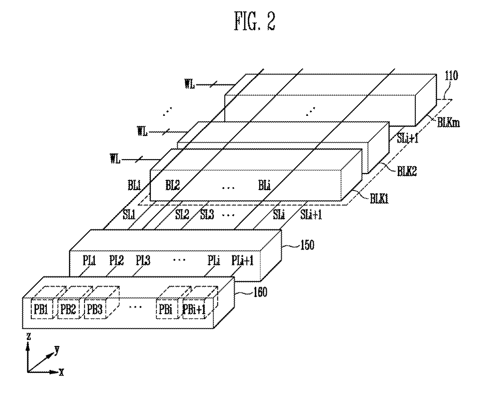
[0023]Hereinafter, various embodiments will be described in detail with reference to the accompanying drawings. The figures are provided to allow those having ordinary skill in the art to understand the scope of the embodiments of the disclosure. The present invention may, however, be embodied in different forms and should not be construed as limited to the embodiments set forth herein. Rather, these embodiments are provided so that this disclosure will be thorough and complete, and will fully convey the scope of the present invention to those skilled in the art. Throughout the disclosure, reference numerals correspond directly to the like parts in the various figures and embodiments of the present invention.

[0024]Furthermore, ‘connected / coupled’ represents that one component is directly coupled to another component or indirectly coupled through another component. In this specification, a singular form may include a plural form as long as it is not specifically mentioned in a senten...


PUM


Abstract

A semiconductor device includes first memory blocks arranged in a longitudinal direction, and including a plurality of strings, wherein the strings are formed along a vertical direction, and the strings adjacent to each other share bit lines or source lines with each other, each string including a drain selection transistor coupled to an odd drain selection line or an even drain selection line, memory cells coupled to word lines, and a source selection transistor coupled to an odd source selection line or an even source selection line, page buffers suitable for storing data, a selection switch unit suitable for transferring the data stored in the page buffers or various voltages supplied from an external source to the bit lines and the source lines; and a control circuit suitable for controlling the page buffers and the selection switch unit.

Description

CROSS-REFERENCE TO RELATED APPLICATION[0001]The present application claims priority to Korean patent application number 10-2013-0084685 filed on Jul. 18, 2013, in the Korean Intellectual Property Office, the entire disclosure of which is incorporated by reference herein.BACKGROUND[0002]1. Technical Field[0003]Various exemplary embodiments relate to a semiconductor device and a method of operating the same, and more particularly, to a semiconductor device having a vertical channel and a method of operating the same.[0004]2. Related Art[0005]An increase in demand of cellular phones, portable memory devices and digital cameras are leading to an increase in demand of non-volatile memory devices that are used mainly as memory devices of these products. Among the non-volatile memory devices, NAND flash memory devices are widely used as data storage devices.[0006]NAND flash memory devices may be classified into two-dimensional (2D) semiconductor devices in which strings are formed in a hor...

Claims


Application Information

Patent Timeline
Patent Type & Authority Patents(United States)
IPC IPC(8): G11C16/04G11C16/10G11C16/16G11C16/24G11C16/26
CPCG11C16/04G11C16/16G11C16/26G11C16/24G11C16/10G11C16/0483G11C16/30G11C16/06
Inventor ARITOME, SEIICHI
Owner SK HYNIX INC
Why Eureka
Try Eureka