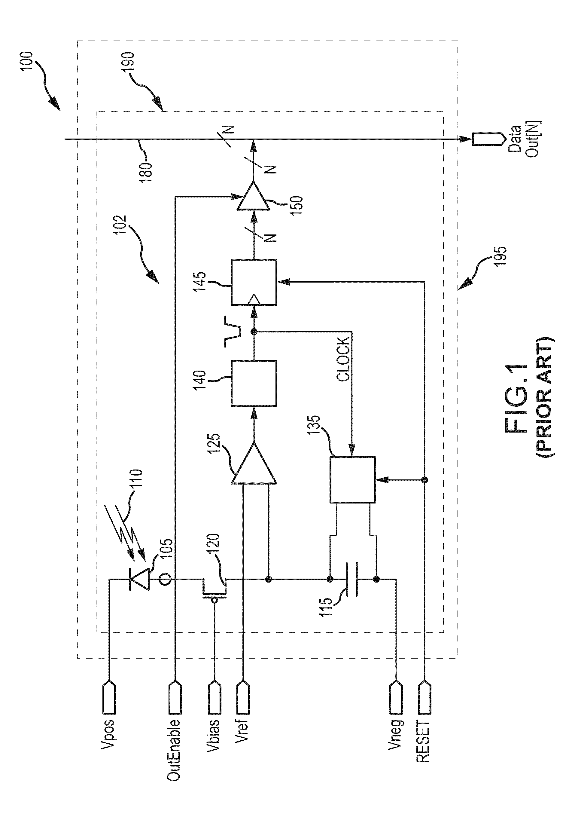
[0016]The Repartitioned Digital Pixel provides a read out circuit for a focal plane array (FPA) of detector elements. The read out circuit comprises an array of pixel cells. Each of the pixel cells includes a storage device (e.g. a capacitor) coupled to a detector element and configured to accumulate a value in response to radiation impinging on the detector element, quantization circuitry configured to compare the accumulated value to a threshold value and generate a quantization event, a logical output configured to report the quantization event and a compensator circuit configured to reduce the accumulated value on the storage device to account for the reported quantization event. The read out circuit further comprises a digital memory (e.g. a counter) disposed physical separated from and coupled to the array of pixel cells. Each of the digital memory locations is in electrical communication with at least one of the pixel cells and configured to store and accumulate a digital value in response to receiving the quantization event from the at least one of the pixel cells. The digital value and accumulated digital value correspond, respectively, to an intensity of the radiation impinging upon the detector element of the at least one of the pixel cells for a given quantization event and for all quantization events over the frame integration interval. One of the novel and enabling aspects of Repartitioned Digital Pixel is that placement of the summing logic in the readout device (as opposed to off-FPA), even if on a different layer of a stacked device, hugely increases the available bandwidth for a given power. This enables the use of shared logic and memory, vs. dedicated accumulators per pixel in other architectures, to accumulate results at speeds consistent with processing individual quantization events. The system cost of implementing the same function and level of performance with off-device logic, as in conventional frame summing, would be highly prohibitive.
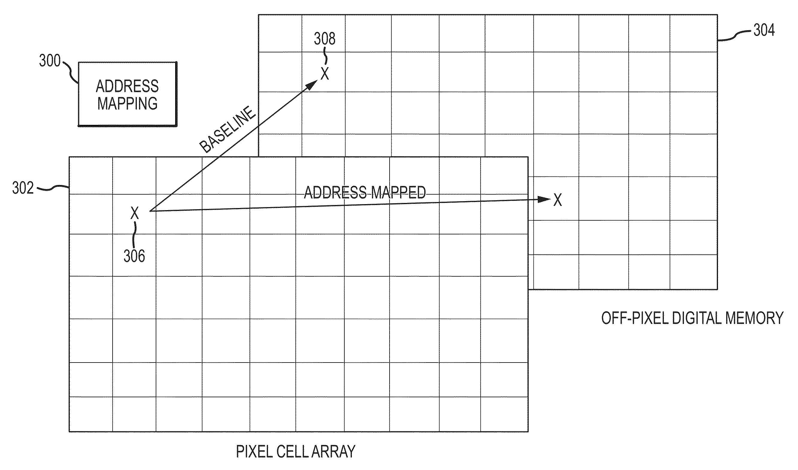
[0017]The present invention introduces an address mapping between the pixel cells and the off-pixel digital memory. In an embodiment, the address mapping is implemented with an address mapping input configured to receive updates to an address-mapping signal during a frame integration interval and a control circuit that is disposed physically separate from the array of pixel cells. The control circuit includes a shared quantization event selector configured to identify the pixels for which a quantization event (asynchronous or synchronous, and with single or multi-bit value) is reported and to initiate memory updates for those pixels. An address generator is configured to determine a memory location for each memory update based on the updated address-mapping signal. Memory update logic is configured to modify the digital value in the corresponding memory location for each memory update. Output logic is configured to output digital values accumulated over the frame integration interval from at least some of the memory locations. The control circuit can implement a generalized address mapping to provide more robust stabilization than orthogonal transfer or TDI. While TDI is typically limited to compensating for displacements in a single axis, and orthogonal transfer extends this to two axes, a generalized address mapping may also include rotation, scaling, and distortion correction. The control circuit may also implement the address mapping by mapping each pixel cell to one of multiple memory locations based on sub-pixel alignments to increase the effective resolution of the detector array.
[0019]In some embodiments, the address mapping is applied to the quantization events. The digital memory comprises quantization memory configured to store and accumulate digital values. The address generator is configured to determine the memory location in the quantization memory for each update. The memory update logic is configured to add the digital value corresponding to the reported quantization event for the pixel cell to the accumulated digital value in the corresponding memory location in the quantization memory for each memory update. The output logic is configured to output the digital values accumulated over the frame integration interval from at least some of the memory locations in the quantization memory. Application of address mapping to the quantization events allows for stabilization at very high update rates, perhaps at or near the native update rate of the detector and the incident radiation. The address mapping for quantization events may be a generalized mapping. In some embodiments, the mapping may be limited to an isomorphic mapping of linear shifts, possibly small linear shifts.
[0021]Application of address mapping to the accumulated sub-frame allows for on-FPA stabilization at sub-frame rates. The address mapping for accumulated sub-frames may be a generalized mapping configured to accommodate small or large shifts, roll, magnification, polynomial warp or keystone correction. In some embodiments, the sub-frame address mapping may be limited to a non-isomorphic mapping that excludes linear shifts. Because quantization events are accumulated before they are further accumulated into a sub-frame, sub-frame motion can be measured a posteriori, before the sub-frame address mapping is applied, avoiding extrapolation error and improving stabilization accuracy.
[0022]In some embodiments, address mapping is applied to both the quantization events and accumulated sub-frames. Address mapping may be applied to the quantization events at a high update rate to align data in the quantization memory as the digital values for reported quantization events are accumulated. This mapping may be confined to small shifts. Address mapping may be applied to the accumulated sub-frames to align data in the frame memory as the accumulated digital values are read out of the quantization memory at a lower sub-frame rate. This mapping may be a generalized mapping. This combination provides robust image stabilization and possibly resolution enhancement.
[0023]In some embodiments, the gain associated with different pixels may be different, and must be compensated before registration and summing. While it is typical to implement this operation as a multiply, this is not necessarily required for quantization event accumulation. A major insight for simplifying the circuit is that, for single-bit events, gain compensation may be achieved by setting the digital value corresponding to a reported quantization event for a given pixel equal to the pixel gain. In essence, the multiply is replaced by addition, as the one-bit events are distributed throughout the registered memory. Multi-bit events may easily be handled via successive addition or simplified few-bit shift-and-add (not typing up DSP slices in an FPGA).

