Optical assembly and method for producing the same

a technology of optical assembly and optical light guide, which is applied in the field of optical assembly, can solve the problems of long time-consuming method for determining the optimal position, and achieve the effect of convenient pre-operation

Active Publication Date: 2015-09-08
SUMITOMO ELECTRIC IND LTD
View PDF26 Cites 0 Cited by
  • Summary
  • Abstract
  • Description
  • Claims
  • Application Information

AI Technical Summary

Benefits of technology

[0010]Another aspect of the present invention relates to a process to manufacture an optical assembly that includes an optical device installing a semiconductor optical device with an active area and a holder having a sleeve to receive the external optical fiber, a skirt to receive the optical device, and a lens put between the sleeve and the skirt, where the sleeve, the skirt, and the lens may be integrally formed with each other. The process of an embodiment may comprise steps of: (a) aligning the optical device in a plane perpendicular to an axis of the lens as inspecting an image of the active area of the semiconductor optical device which is projected on a target surface formed in a deep end of the sleeve; and (b) fixing the optical device with the skirt of the holder. A feature of the process according to an embodiment is that the target surface may include at least two aiming indices to indicate the axis of the lens. Aligning the center of the image focused on the target surface with the axis of lens, the optical alignment between the optical device and the holder in a plane perpendicular to the axis of the lens may be precisely and easily preformed.

Problems solved by technology

The method to produce the optical assembly disclosed in the latter prior art is not only necessary to activate the semiconductor device practically and to prepare an apparatus to monitor the amplitude of the light, but the method takes a long time to determine the optimal position.

Method used


Image

  • Optical assembly and method for producing the same
  • Optical assembly and method for producing the same
  • Optical assembly and method for producing the same

Examples


Embodiment Construction

[0027]Next, some preferred embodiments according to the present invention will be described as referring to drawings. In the description of the drawings, the same numerals or symbols will refer to the same or like elements without overlapping explanations.

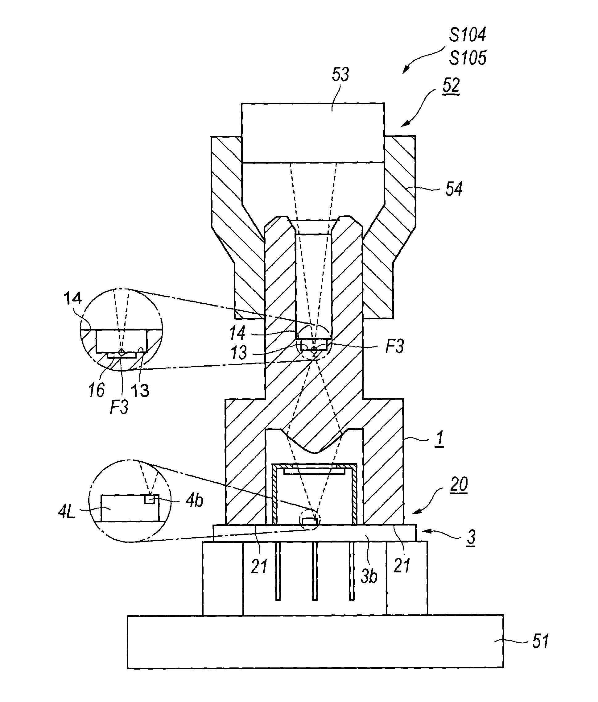
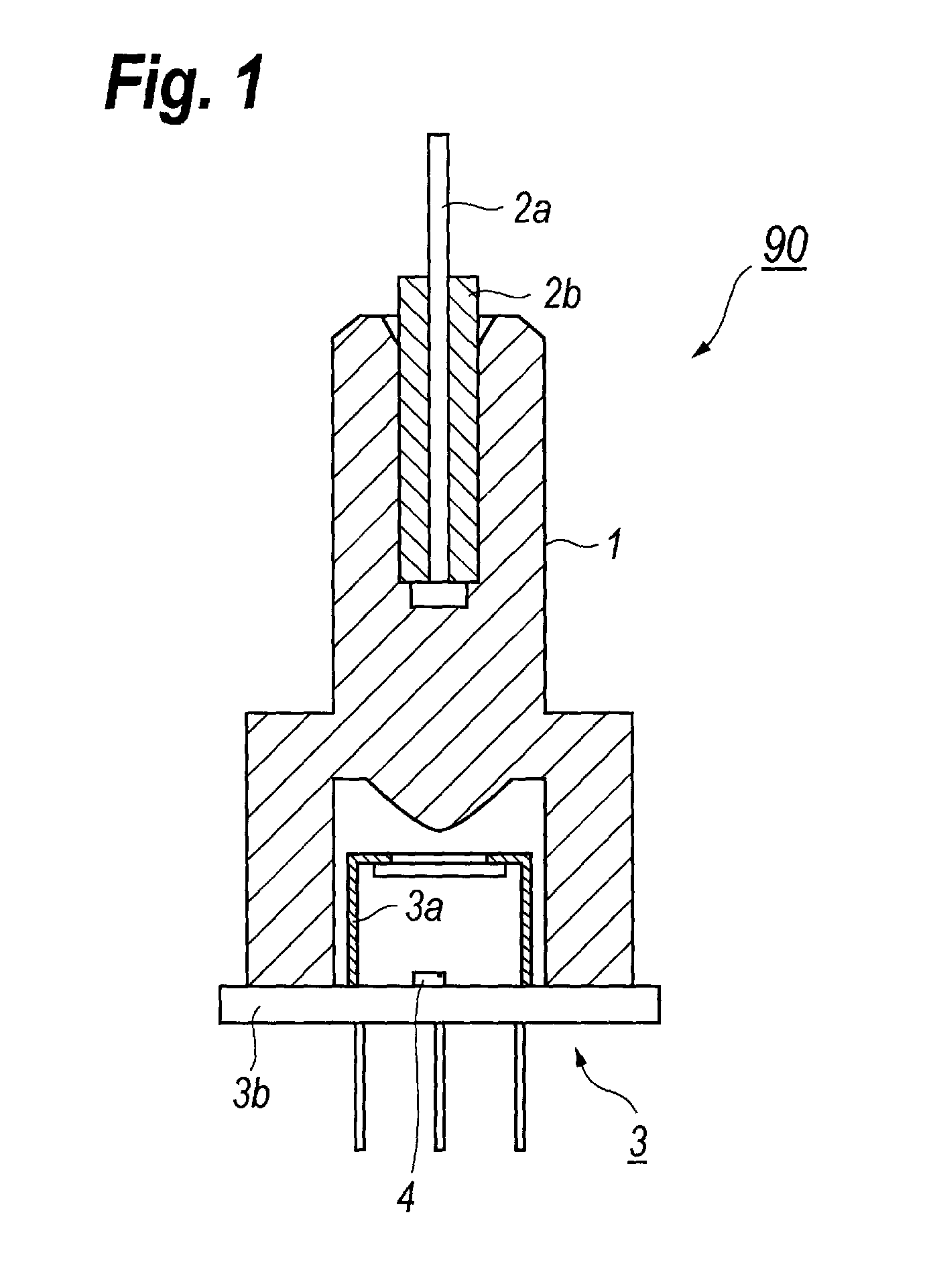
[0028]FIG. 1 shows a cross section of an optical assembly 90 implementing with a holder 1. The optical assembly 90 includes an optical device 3 that installs a semiconductor optical device 4 therein. The optical device 3 includes a cap 3a and a base 3b for mounting the semiconductor optical device 4 thereon. The holder 1 receives in an end thereof an external optical fiber 2a with a ferrule 2b for securing a tip end of the optical fiber. The holder 1 may couple the semiconductor device 4 optically with the external optical fiber 2a. The external optical fiber 2a may be, what is called, a multi-mode fiber.

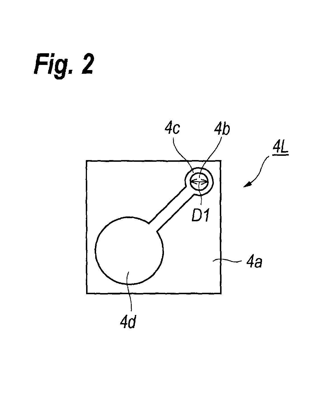
[0029]The semiconductor optical device 4 may be, for instance, a laser diode (LD), or a photodiode (PD). The embodiment shown in ...


PUM

PropertyMeasurementUnit
inspecting wavelengthaaaaaaaaaa
wavelengthaaaaaaaaaa
diameteraaaaaaaaaa

Abstract

An optical assembly is disclosed where the optical assembly provides an optical device and a holder including a sleeve, a skirt, and a lens. The sleeve has a bore, into which an external optical fiber is set to couple with the optical device, providing a target surface in an end thereof. The target surface includes an aiming index to indicate the axis of the lens.

Description

TECHNICAL FIELD[0001]An embodiment of the present invention relates to an optical assembly, in particular, relates to an optical assembly including an optical device and a holder integrating a receptacle, a skirt and a lens. An embodiment of the invention further relates to a method to produce the optical assembly.BACKGROUND ART[0002]A recent communicating system has continuously requested the higher speed and the greater capacity. An optical assembly that includes a semiconductor optical device, such as a laser diode (LD) for emitting light or a photodiode (PD) for receiving light, and a mechanism to couple the semiconductor optical device with an external optical fiber is widely applied in the optical communication system. The optical device often has, what is called, a CAN package, while, the coupling mechanism includes a sleeve to receive the external optical fiber, a skirt to receive the CAN package and a lens integrally formed with the sleeve and the skirt.[0003]A Japanese Pat...

Claims


Application Information

Patent Timeline
Patent Type & Authority Patents(United States)
IPC IPC(8): G02B6/42
CPCG02B6/42G02B6/4204G02B6/4224Y10T29/49895
Inventor NISHIE, MITSUAKIMURATA, MICHIONAKANISHI, HIROMI
Owner SUMITOMO ELECTRIC IND LTD
Why Eureka
Try Eureka