
Differential sense amplifier without switch transistors

a technology of switch transistors and sense amplifiers, applied in the field of sense amplifiers, can solve the problems of increasing the area of the entire circuit and its fabrication cost, and achieve the effect of simple and robust memory sense amplifiers

Active Publication Date: 2015-09-15
SOITEC SA
View PDF12 Cites 8 Cited by
  • Summary
  • Abstract
  • Description
  • Claims
  • Application Information

AI Technical Summary

Benefits of technology

[0020]The present invention relates to a simplified and robust memory sense amplifier. According to a first aspect, a differential sense amplifier for sensing data stored in a plurality of memory cells of a memory cell array, including:

Problems solved by technology

Although sense amplifiers are technically necessary, from an economical point of view the sense amplifiers can be considered as service circuits of the memory array and therefore as overhead that increases the area of the entire circuit and thus also its cost of fabrication.

Method used


Image

  • Differential sense amplifier without switch transistors
  • Differential sense amplifier without switch transistors
  • Differential sense amplifier without switch transistors

Examples


first embodiment

No Switch Transistors

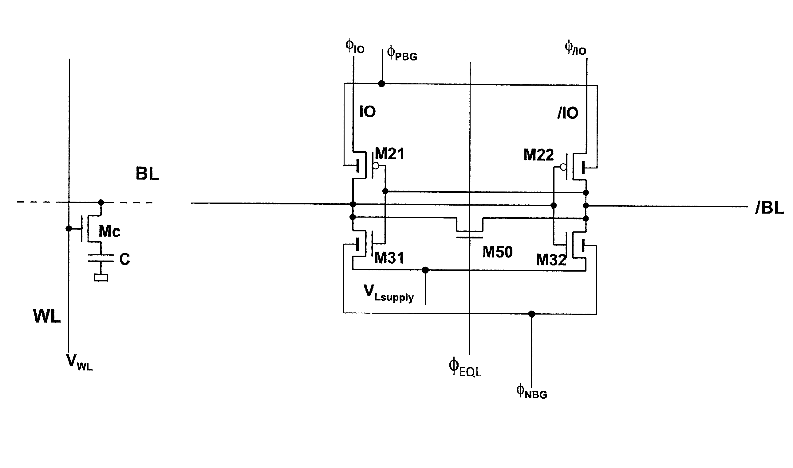
[0090]As illustrated in FIG. 3, a sense amplifier according to the first embodiment of the invention includes four transistors M21, M22, M31, M32 for the inverters, with two additional pass-gate transistors M71, M72, two additional precharge transistors M61, M62 and one additional equalization transistor M50.

[0091]As for FIG. 1 illustrating a prior art sense amplifier, and for simplicity's sake, only one word line WL and one memory cell C are shown on the left hand side of the sense amplifier. The cell C is addressed by the word line WL that controls the gate of a cell access transistor Mc, the cell access transistor Mc connecting the memory cell C to a bit line.

[0092]The differential sense amplifier for sensing data stored in a plurality of memory cells C of a memory cell array according to the first embodiment comprises:[0093]a first CMOS inverter having an output connected to a first bit line BL and an input connected to a second bit line / BL complementary to...

second embodiment

No Switch Transistors and No Dedicated Precharge Transistors

[0139]As illustrated in FIG. 5, a sense amplifier according to a second embodiment of the invention includes four transistors M21, M22, M31, M32 for the inverters, with two additional dedicated pass-gate transistors M71, M72 and one additional equalization transistor M50.

[0140]The second embodiment is similar to the first embodiment except for the further absence of dedicated precharge transistors. Therefore, only the differences between the two embodiments are described.

[0141]Compared to the first embodiment, the precharge operation is performed by the pull-up transistors M21, M22 or by the pull-down transistors M31, M32. Hence the precharge transistors are constituted by the pull-up transistors M21, M22 or by the pull-down transistors M31, M32. Dedicated precharge transistors M61, M62 as shown in FIG. 3 are thus omitted in this second embodiment, so is the corresponding precharge control signal φPCH.

Operating Process of a...

third embodiment

No Switch Transistors and No Dedicated Pass-Gate Transistors

[0150]As illustrated in FIG. 7, a sense amplifier according to a third embodiment of the invention includes four transistors M21, M22, M31, M32 for the inverters, with two additional dedicated precharge transistors M61, M62 and one additional equalization transistor M50.

[0151]The third embodiment is similar to the first embodiment except for the further absence of dedicated pass-gate transistors. Therefore, only the differences between the two embodiments are described.

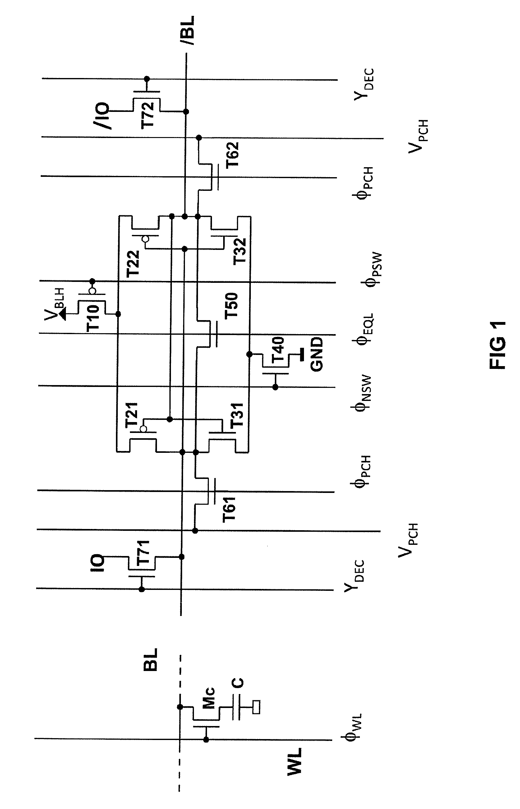
[0152]Compared to the first embodiment, the read operation is performed by the pull-up transistors M21, M22 or by the pull-down transistors M31, M32. Hence the pass-gate transistors are constituted by the pull-up transistors M21, M22 or by the pull-down transistors M31, M32. Dedicated pass-gate transistors T71, T72 as shown in FIG. 1 are thus omitted in this third embodiment, so is the corresponding decoding control signal YDEC. The pass-gate transistors cons...


PUM


Abstract

A differential sense amplifier for sensing data stored in a plurality of memory cells of a memory cell array, including a first CMOS inverter having an output connected to a first bit line (BL) and an input connected to a second bit line complementary to the first bit line and a second CMOS inverter having an output connected to the second bit line ( / BL) and an input connected to the first bit line. Each CMOS inverter includes pull-up and pull-down transistors, wherein the sources of either of the pull-up transistors or the pull-down transistors are electrically coupled and connected to a pull-up voltage source or a pull-down voltage source without an intermediate transistor between the sources of the transistors and the voltage source.

Description

[0001]This application is related to U.S. patent application Ser. No. 13 / 456,047, entitled “Differential Sense Amplifier Without Dedicated Pass-Gate Transistors,” which was filed on Apr. 25, 2012.FIELD OF THE INVENTION[0002]The invention generally relates to semiconductor memories, and more particularly to a sense amplifier for sensing data stored in a plurality of memory cells of a memory cell array.BACKGROUND OF THE INVENTION[0003]Semiconductor memories are used in computers, servers, handheld devices such as cell phones etc., printers, and many further electronic devices and applications. A semiconductor memory comprises a plurality of memory cells in a memory array, each memory cell storing at least a bit of information. Dynamic Random Access Memories (DRAMs) are an example of such semiconductor memories. The present invention is preferably embodied with DRAMs. As a consequence, the following description is done with reference to a DRAM as a non limiting example.[0004]A sense am...

Claims


Application Information

Patent Timeline
Patent Type & Authority Patents(United States)
IPC IPC(8): G11C7/12G11C7/02G11C7/06G11C11/4094G11C11/4091
CPCG11C7/065G11C7/12G11C11/4091G11C11/4094G11C2211/4016G11C2207/002
Inventor FERRANT, RICHARDTHEWES, ROLAND
Owner SOITEC SA
Learn More