Display device, liquid crystal display device and electronic device including the same

a technology of liquid crystal display and display device, which is applied in the field of display devices, can solve the problems of increasing costs, and affecting reliability, and achieves the suppression of poor connection between the connection portion of the panel and the external component, preventing heat generation or an increase in power consumption due to reading a look-up table from a memory element, and reducing the yield of display devices

Inactive Publication Date: 2015-09-22
SEMICON ENERGY LAB CO LTD
View PDF81 Cites 6 Cited by
  • Summary
  • Abstract
  • Description
  • Claims
  • Application Information

AI Technical Summary

Benefits of technology

[0010]Alternatively, in order to read the signals corresponding to the respective subpixels from a memory element in which the look-up table is stored, the memory element needs to be driven at high speed. Therefore, as the look-up table is read from the memory element, heat is generated, whereby power consumption is increased in some cases. Alternatively, since the memory element for storing the look-up table is needed, a cost is increased. Alternatively, a pathway from generating the signals corresponding to the respective subpixels to writing the signals to the respective subpixel is long, and a connection portion of the panel and the external component exists in the course of the pathway. Therefore, the signals are likely to be influenced by noise and display quality is decreased, which is a problem.
[0063]According to one embodiment of this invention, since one digital signal can be converted into a plurality of analog signals, a look-up table can be unnecessary. Therefore, heat generation or an increase in power consumption due to reading a look-up table from a memory element can be prevented. Alternatively, since signals corresponding to respective subpixels can be generated on a panel, the number of connection between the panel and an external component can be small. Alternatively, poor connection in the connection portion of the panel and the external component can be suppressed, whereby reliability can be increased. Alternatively, an yield in production of a display device can be increased. Alternatively, a production cost of the display device can be reduced. Alternatively, since the number of connection between the panel and the external component can be reduced, a high-definition display portion can be obtained. Alternatively, since the number of connection between the panel and the external component can be reduced, resistance to noise can be enhanced and display quality can be increased.

Problems solved by technology

As a result, poor connection is generated in a connection portion between the panel and the external component, whereby a problem of decrease in reliability is concerned.
Alternatively, an yield in production of the display device is decreased, whereby a problem of an increase in a cost is concerned.
Alternatively, the number of connection between the panel and the external component is increased, whereby a problem in that it is difficult to obtain a high-definition display device is concerned.
Accordingly, a problem in that it is difficult to form a part for generating the signals corresponding to the respective subpixels and the pixel over the same substrate is concerned.
Therefore, as the look-up table is read from the memory element, heat is generated, whereby power consumption is increased in some cases.
Alternatively, since the memory element for storing the look-up table is needed, a cost is increased.
Therefore, the signals are likely to be influenced by noise and display quality is decreased, which is a problem.

Method used


Image

  • Display device, liquid crystal display device and electronic device including the same
  • Display device, liquid crystal display device and electronic device including the same
  • Display device, liquid crystal display device and electronic device including the same

Examples


embodiment 1

(Embodiment 1)

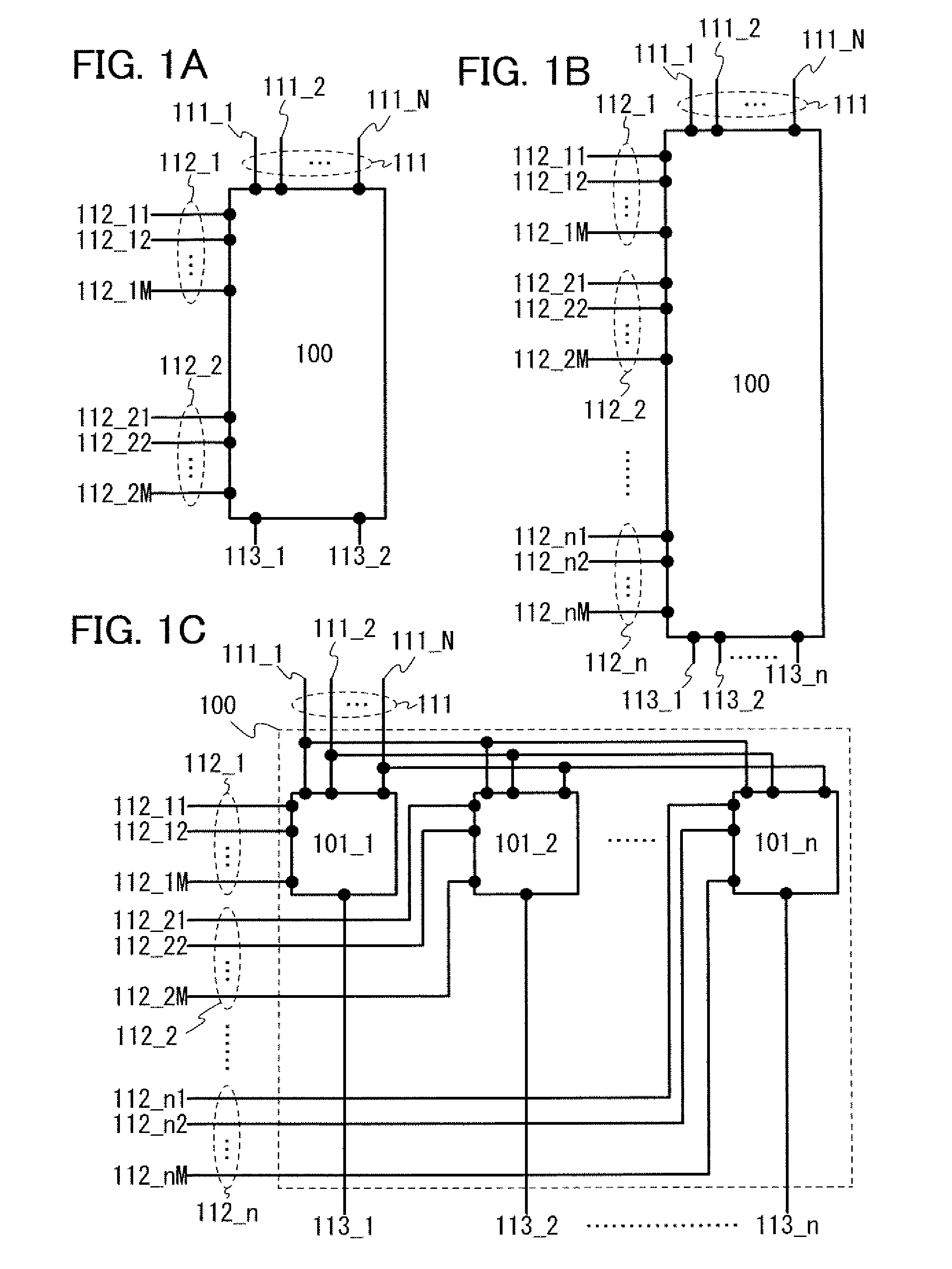
[0086]In this embodiment, a digital-analog converter portion will be described. The digital-analog converter portion of this embodiment converts one digital signal (e.g., a digital signal with N bits (N is a natural number of 2 or more)) into n (n is a natural number of 2 or more) analog signals. In order to realize this, n groups (e.g., voltage groups or current groups) are input to the digital-analog converter portion. Note that a structure in which some of the respective groups input to the digital-analog converter portion can be used as one in common is possible. In this case, less than n groups are input to the digital analog converter portion.

[0087]Note that the values (e.g., voltage or current) of the n analog signals are different from each other However, some of the n analog signals have the same value in some cases. Alternatively, all the values of the n analog signals are the same in some cases. For example, in the case of a digital signal with the maximum o...

embodiment 2

(Embodiment 2)

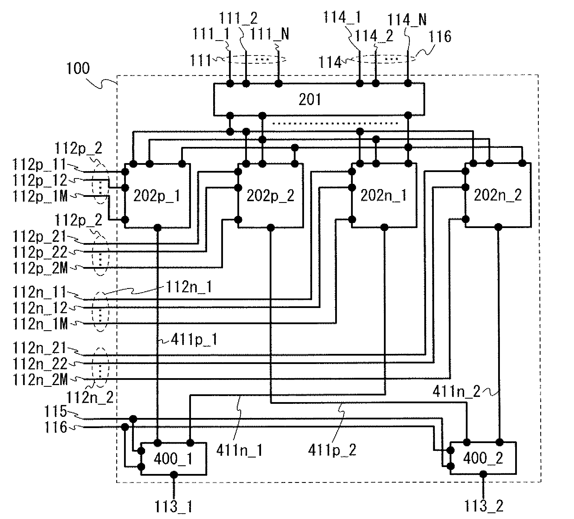
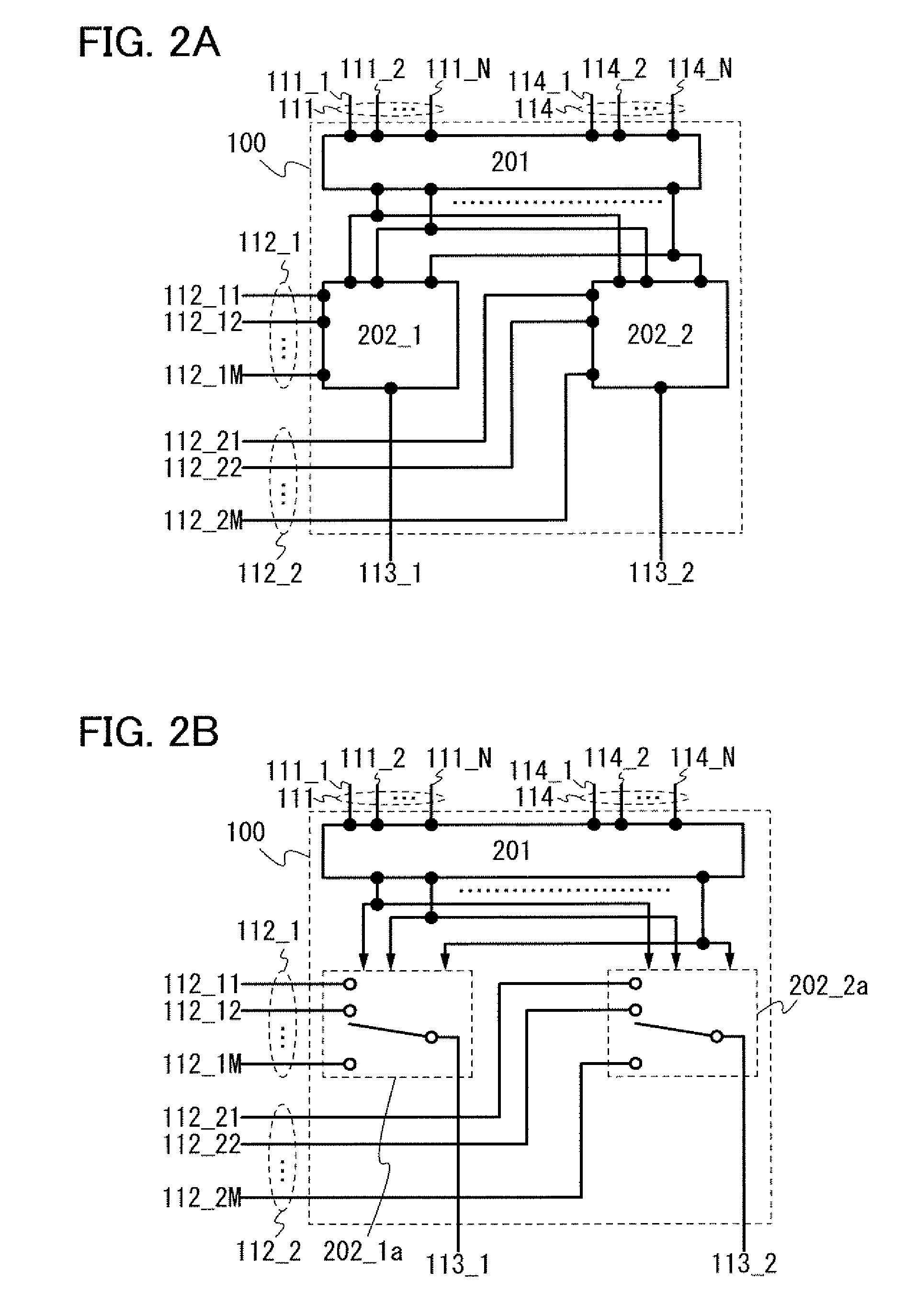
[0138]In this embodiment, one example of the digital-analog converter portion 100 in which one digital signal is converted into two analog signals as shown in FIG. 1A will be described with reference to FIG. 2A.

[0139]The digital-analog converter portion 100 includes a circuit 201, a circuit 202_1, and a circuit 202_2.

[0140]The circuit 201 is connected to the wiring group 111 and a wiring group 114. The circuit 202_1 is connected to the wiring group 112_1, the wiring 113_1, and an output terminal of the circuit 201. The circuit 202_2 is connected to the wiring group 112_2, the wiring 113_2, and the output terminal of the circuit 201.

[0141]The wiring group 114 includes a plurality of wirings. For example, the wiring group 114 includes N wirings of wirings 114_1 to 114_N.

[0142]An inverted digital signal is input to the wiring group 114. Therefore, the number of bits of the inverted digital signal corresponds to the number of wirings in the wiring group 114 in many cases. ...

embodiment 3

(Embodiment 3)

[0206]In this embodiment, one example of the digital-analog converter portion 100 which can separately set the polarity of each analog signal will be described with reference to FIG. 6A.

[0207]In order to separately set the polarity of each analog signal, for example, the digital-analog converter portion 100 has a first mode and a second mode. Even when the digital signals with N bits are input, the values (polarities) of the analog signals are different from each other in the first mode and the second mode in many cases.

[0208]For example, each analog signal has a positive potential in the first mode and has a negative potential in the second mode. Accordingly, the polarity of each analog signal can be separately set. However, this embodiment is not limited to this. The values and the polarities of the analog signals are the same in the first mode and the second mode in some cases. Alternatively, the values of the analog signals can be different from each other in the f...


PUM


Abstract

A liquid crystal display device includes a pixel having a first to nth (n is a natural number of 2 or more) subpixels and a circuit. To the circuit N (N is a natural number of 2 or more) wirings for supplying a digital signal with N bits and first to nth wiring groups having M (M is a natural number of 2 or more) wirings for supplying M different voltages are electrically connected. The liquid crystal display device has a function of converting the digital signal into n analog signals by using the M voltages supplied to the first to nth wiring groups and inputting the n analog signals to first to nth subpixels. The first to nth subpixels each include an electrode for driving a liquid crystal element.

Description

BACKGROUND OF THE INVENTION[0001]1. Field of the Invention[0002]One embodiment of this invention relates to a display device or a driving method of the display device. In specific, one embodiment of this invention relates to a liquid crystal display device in which a pixel is divided into a plurality of subpixels and a driving method of the liquid crystal display device. Further, one embodiment of this invention relates to a liquid crystal display device or an electronic device including the liquid crystal display device in a display portion.[0003]2. Description of the Related Art[0004]Liquid crystal display devices are used for a variety of electronic products such as cell phones and television receiver and many research is conducted for further improvement in the quality.[0005]While advantages of a liquid crystal display device are small size, light weight, and low power consumption compared to a CRT (cathode-ray tube) and, a problem of the liquid crystal display device is the nar...

Claims


Application Information

Patent Timeline
Patent Type & Authority Patents(United States)
IPC IPC(8): G06F3/038G09G3/36
CPCG09G3/3688G09G3/3696G09G2310/027G09G2320/068G09G2320/0673G09G3/3413G09G3/3607G09G3/3655G09G2330/023
Inventor KIMURA, HAJIMEUMEZAKI, ATSUSHI
Owner SEMICON ENERGY LAB CO LTD
Why Eureka
Try Eureka