Exposure apparatus and device manufacturing method using original with phase-modulation diffraction grating to form interference pattern
a technology of phase modulation diffraction grating and manufacturing method, applied in the field of exposure apparatus, can solve the problems of local defects of the final pattern, unwanted interference pattern called speckle, etc., and achieve the effect of reducing the influence of speckles and simple arrangemen
- Summary
- Abstract
- Description
- Claims
- Application Information
AI Technical Summary
Benefits of technology
Problems solved by technology
Method used
Image

Examples
first embodiment
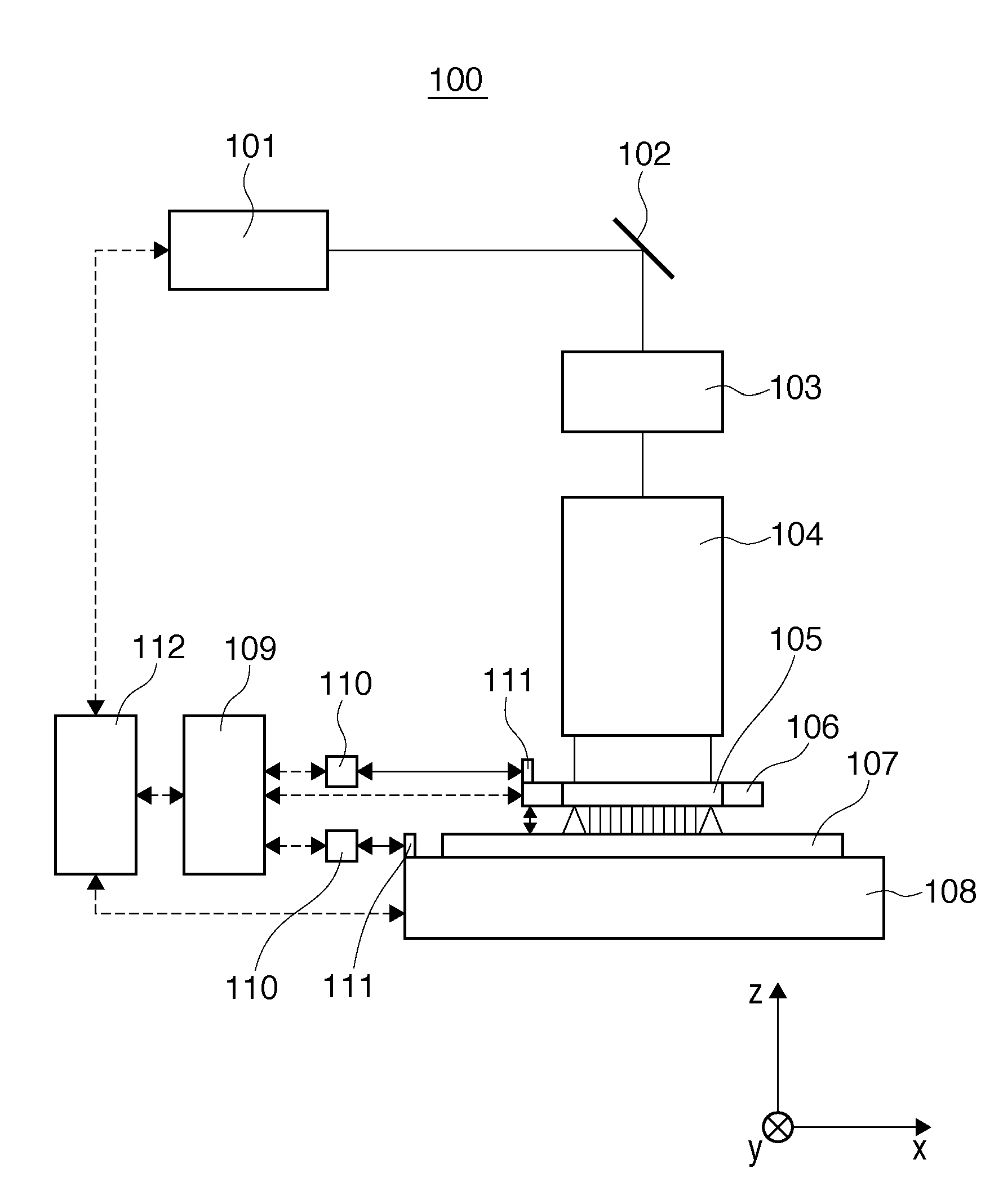
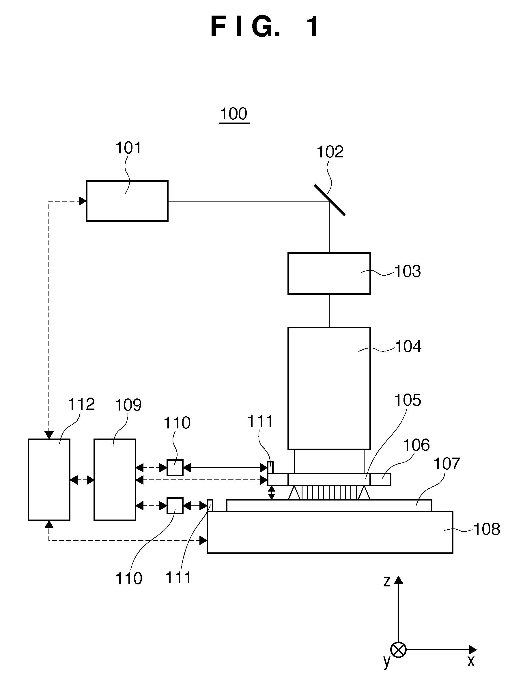
[0019]FIG. 1 is a view schematically showing the arrangement of an exposure apparatus 100 according to the first embodiment of the present invention. Throughout this specification and the accompanying drawings, the directions are represented by an x-y-z coordinate system in which the scanning direction of an exposure target substrate is the y direction, the direction of the normal to the surface of the substrate is the z direction, and a direction perpendicular to the y and z directions is the x direction.
[0020]The exposure apparatus 100 includes a light source 101, reflecting mirror 102, light beam dividing optical system 103, beam shaping optical system 104, original holding unit 106, substrate stage (substrate holding unit) 108, measurement unit 109, and control unit 112.
[0021]The light source 101 can include, for example, a mercury lamp, semiconductor laser, solid-state laser, gas laser, or excimer laser. Although a light beam emitted by the light source 101 enters the light bea...
second embodiment
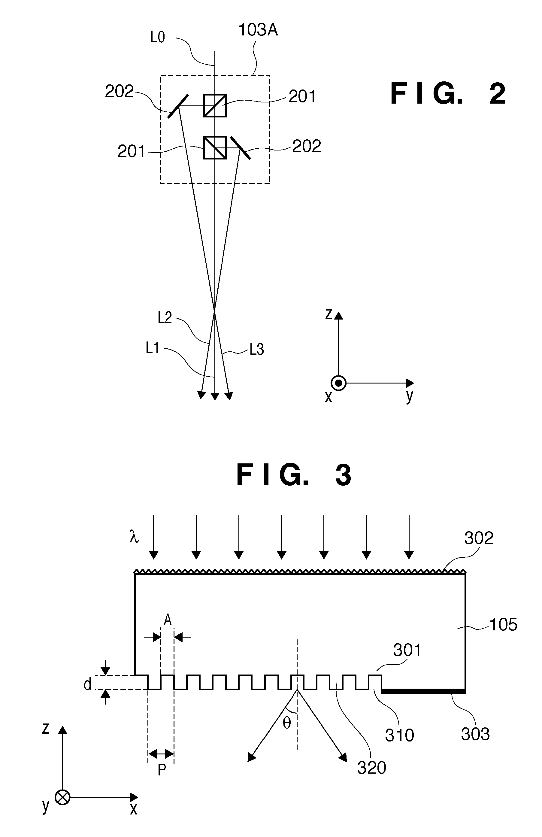
[0052]Points of difference from the exposure apparatus according to the first embodiment will be explained. Details which are not particularly referred to herein can be the same as in the first embodiment. FIG. 7 is a view showing the schematic arrangement of a light beam dividing optical system in an exposure apparatus according to the second embodiment of the present invention. In the second embodiment, of the optical paths of a plurality of light beams (in this embodiment, a reflected light beam and a transmitted light beam) split by a beam splitter 201, that of at least one light beam (in this embodiment, the reflected light beam) is extended to give an optical path length difference from other light beams to the at least one light beam. This optical path length difference can be given by, for example, a plurality of reflecting mirrors 701, as illustrated in FIG. 7.
[0053]A light beam L0 enters a light beam dividing optical system 103B, shown in FIG. 7, as one example of the ligh...
third embodiment
[0057]A light beam direction controller which periodically deflects a light beam so that it is scanned within a set range may be provided. Periodically deflecting a light beam which enters an original by the light beam direction controller makes it possible to reduce the influence of speckle noise generated on a targeted interference pattern. This effect can be achieved by providing, for example, a driving mechanism which drives a reflecting mirror which constitutes a light beam dividing optical system 103.
PUM
| Property | Measurement | Unit |
|---|---|---|
| transparent | aaaaa | aaaaa |
| refractive index | aaaaa | aaaaa |
| depth | aaaaa | aaaaa |
Abstract
Description
Claims
Application Information
 - R&D
- Intellectual Property
- Life Sciences
- Materials
- Tech Scout
- Unparalleled Data Quality
- Higher Quality Content
- 60% Fewer Hallucinations
Browse by: Latest US Patents, China's latest patents, Technical Efficacy Thesaurus, Application Domain, Technology Topic, Popular Technical Reports.
© 2025 PatSnap. All rights reserved.Legal|Privacy policy|Modern Slavery Act Transparency Statement|Sitemap|About US| Contact US: help@patsnap.com