Edge launch transition for a printed circuit board

a technology of printed circuit board and launch transition, which is applied in the direction of printed circuit assembling, cross-talk/noise/interference reduction, printed circuit aspects, etc., can solve the problems of reducing the tolerance of mounting edge irregularities or angular misalignment, and establishing high-quality microwave/mmw connections by means of coaxial connectors at frequencies beyond 20 ghz, etc., to achieve the effect of improving the tolerance of mounting edge irregularities or angular mis

Active Publication Date: 2015-10-27
HITTITE MICROWAVE LLC
View PDF5 Cites 15 Cited by
  • Summary
  • Abstract
  • Description
  • Claims
  • Application Information

AI Technical Summary

Benefits of technology

[0014]In another embodiment, a method provides an edge launch transition for connecting a connector to a printed circuit board having a plurality of ground planes on or within the printed circuit board. The method includes providing an elongated edge on a first edge of the printed circuit board; providing an elongated edge-plated region by disposing an edge plating on the elongated edge to connect the plurality of ground planes; and providing on the printed circuit board an edge launch on a second edge extending outwardly beyond the first edge for providing a well-defined, reproducible RF ground path from the connector to the printed circuit board with improved tolerance to mounting edge irregularities or angular misalignment between the connector and the printed circuit board. Providing the elongated edge may include routing the elongated edge.

Problems solved by technology

However, establishing high quality microwave / mmW connections by means of coaxial connectors becomes difficult at frequencies beyond 20 GHz due to certain fundamental problems manifesting themselves as parasitics at the very area of transition from the planar type of transmission line on the PCB or other substrate to the coaxial type of transmission line, such as a coaxial connector.
The former approach to implement a planar to coaxial transition has limited use at higher frequencies due to inherent parasitic inductance of the ground vias connecting the ground planes on the top and bottom of the printed circuit boards as well as the internal ground planes in multilayer printed circuit boards.
This removal of dielectric material may lead to degradation of the performance at frequencies beyond 30 GHz due to parasitic inductance.
This may somewhat reduce the parasitic inductance of the via holes, but, due to the fact that elongated vias cannot be drilled, but rather must be routed or machined, the routing diameter of the elongated vias must be substantially greater than the diameter of drilled round vias, such that the remaining portions of the conductor deposited in the elongated vias cannot be placed very close to the microstrip launch area.

Method used


Image

  • Edge launch transition for a printed circuit board
  • Edge launch transition for a printed circuit board
  • Edge launch transition for a printed circuit board

Examples


Embodiment Construction

[0032]Aside from the preferred embodiment or embodiments disclosed below, this invention is capable of other embodiments and of being practiced or being carried out in various ways. Thus, it is to be understood that the invention is not limited in its application to the details of construction and the arrangements of components set forth in the following description or illustrated in the drawings. If only one embodiment is described herein, the claims hereof are not to be limited to that embodiment. Moreover, the claims hereof are not to be read restrictively unless there is clear and convincing evidence manifesting a certain exclusion, restriction, or disclaimer.

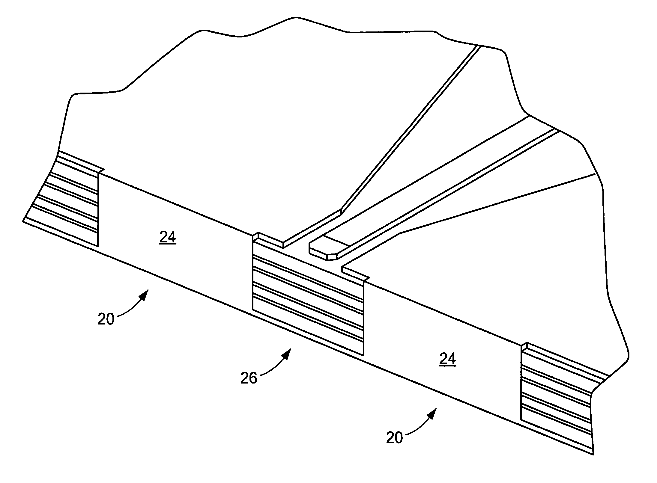
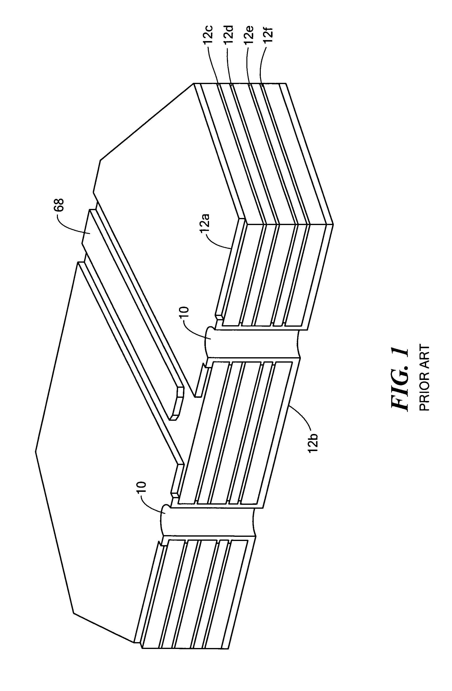
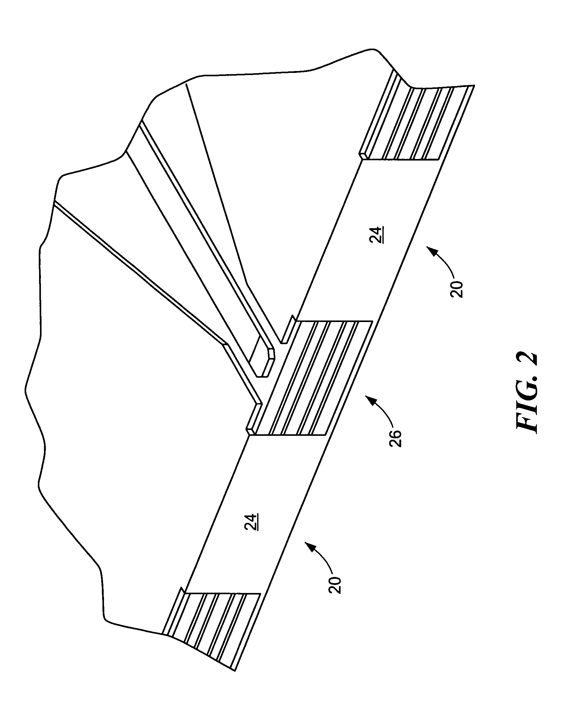
[0033]One former approach to implement a planar to coaxial transition has limited use at higher frequencies due to inherent parasitic inductance of the ground vias, 10FIG. 1, connecting the ground planes 12a and 12b on the top and bottom of the printed circuit boards as well as the internal ground planes 12c-12f in multilay...


PUM


Abstract

An edge launch and fabrication method wherein spaced elongated slots are formed through a circuit board. The slots are plated at least along one side thereof connecting ground planes of the circuit board thus forming spaced edge plated regions. Circuit modules are produced by singulating the circuit board along a cut line offset outwardly from the plated slot sides to form an edge launch outwardly extending from and between the spaced edge plated regions.

Description

RELATED APPLICATIONS[0001]This application claims benefit of and priority to U.S. Provisional Application Ser. No. 61 / 464,942 filed Mar. 11, 2011 under 35 U.S.C. §§119, 120, 363, 365, and 37 C.F.R. §1.55 and §1.78 which is incorporated herein by this reference.FIELD OF THE INVENTION[0002]This invention relates to printed circuit boards and the connections made thereto.BACKGROUND OF THE INVENTION[0003]A printed circuit board (PCB) that includes printed transmission lines such as microstrip or grounded-coplanar with associated ground planes not only provides compact and lightweight circuits, but also provides broadband frequency capabilities.[0004]However, establishing high quality microwave / mmW connections by means of coaxial connectors becomes difficult at frequencies beyond 20 GHz due to certain fundamental problems manifesting themselves as parasitics at the very area of transition from the planar type of transmission line on the PCB or other substrate to the coaxial type of trans...

Claims


Application Information

Patent Timeline
Patent Type & Authority Patents(United States)
IPC IPC(8): H05K1/11H05K3/32
CPCH05K1/117H05K3/32H05K1/0219H05K1/025H05K2201/09181H05K2201/09336H05K2201/09727H05K2201/10189H05K2201/10446
Inventor SOKOL, SERGEYORAN, EKREM
Owner HITTITE MICROWAVE LLC
Why Eureka
Try Eureka