

Substrate etching method and substrate processing device
a substrate and processing device technology, applied in the field of microelectronics technology, can solve the problems of difficult control of sidewall morphology, unsatisfactory product result of such an etching, and uneven sidewall of etched section, so as to increase the process quality of substrate, stable state rapidly, and increase the effect of process performan
- Summary
- Abstract
- Description
- Claims
- Application Information
AI Technical Summary
Benefits of technology
Problems solved by technology
Method used
Image

Examples
Embodiment Construction
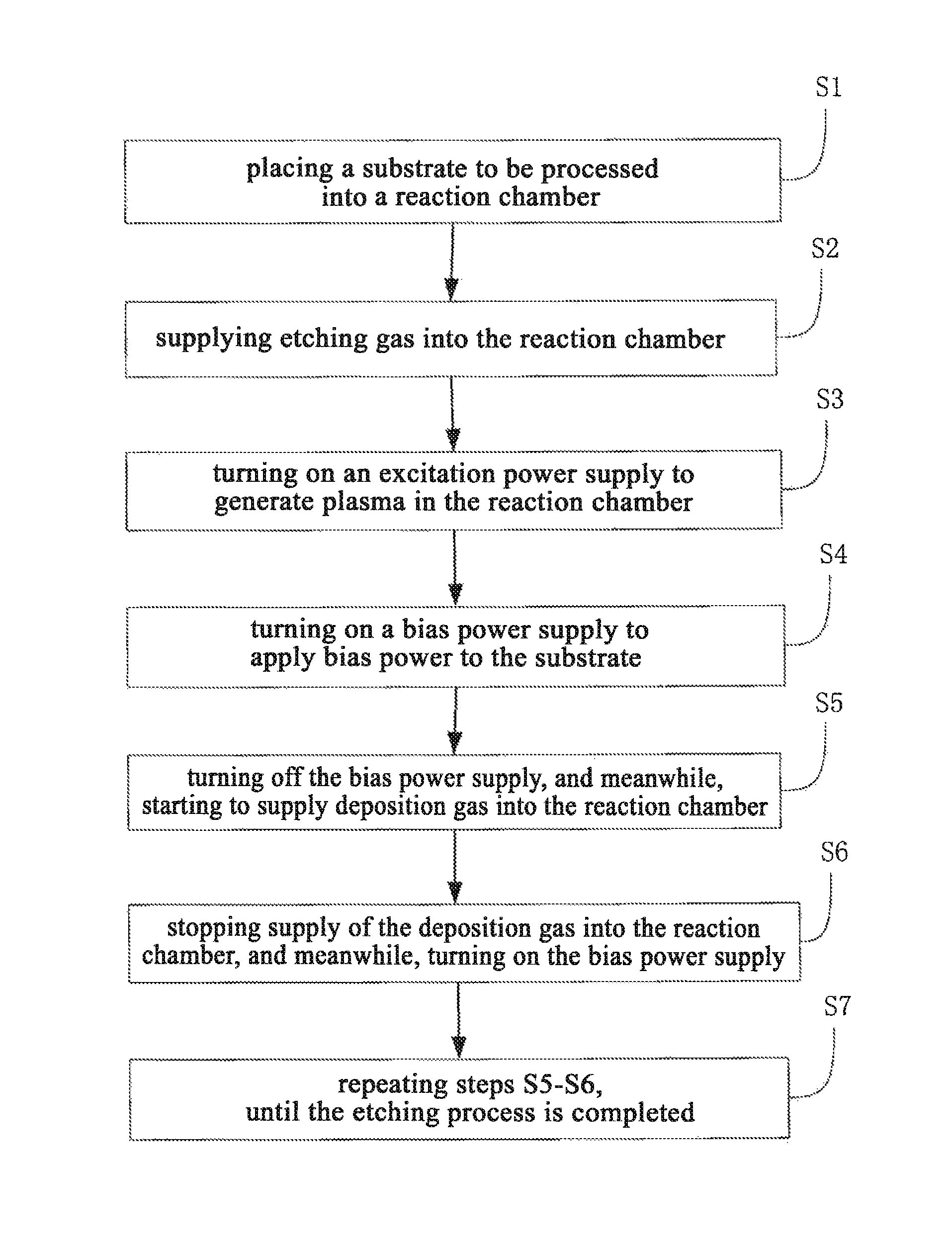
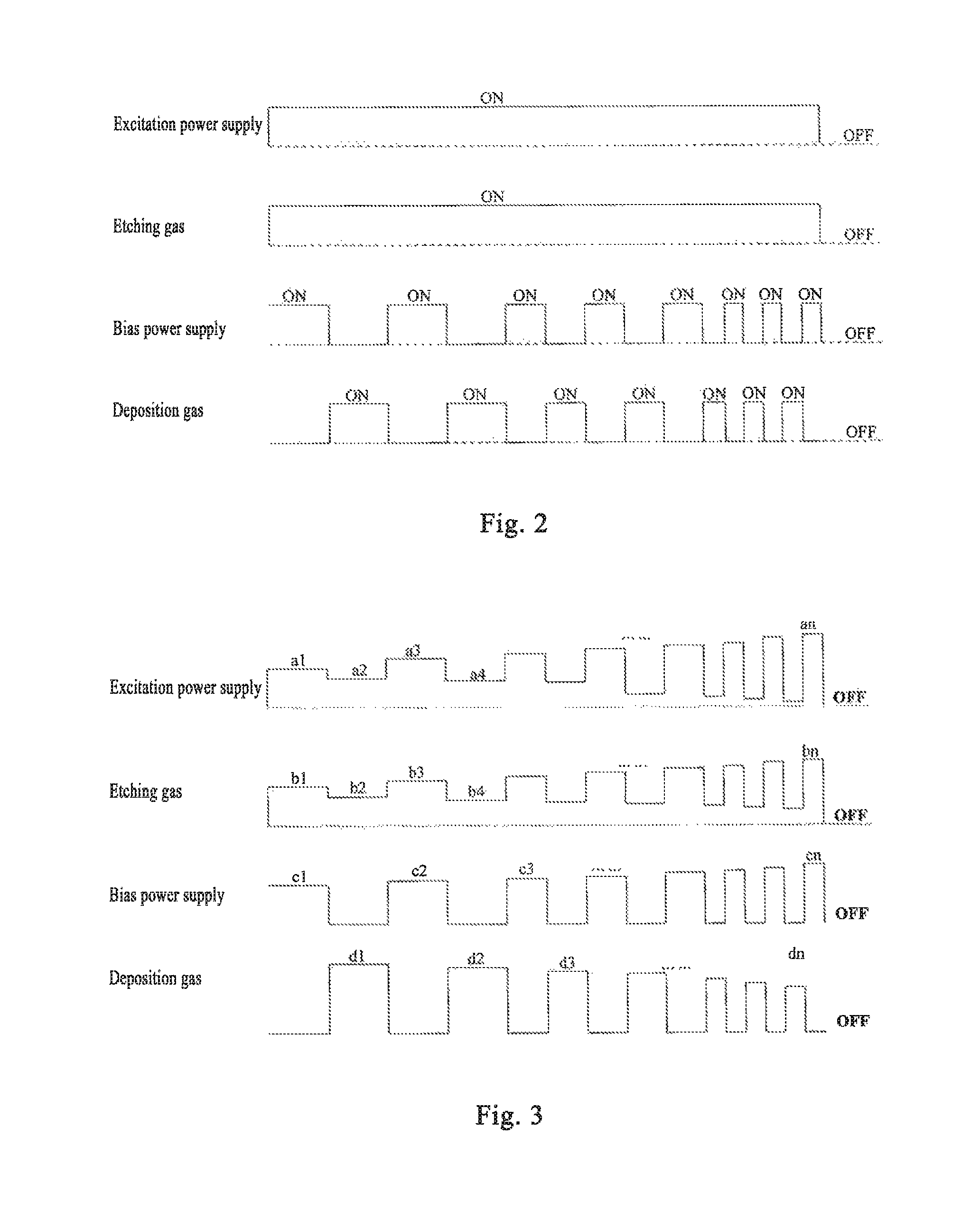
[0035]The following will describe embodiments of the invention in detail and examples of the embodiments are illustrated in the accompanying drawings, wherein like or similar reference numerals indicate like or similar elements or elements with like or similar functions throughout the description. The embodiments described below referring to the drawings are exemplary, are only used to explain the invention and are not intended to limit the invention.
[0036]The following disclosure provides various embodiments or examples to implement various structures of the invention. In order to simply the disclosure, components and configurations of specific examples will be described in the following. Of course, they are merely examples and are not intended to limit the invention. In addition, the invention may refer to numbers and / or letters repeatedly in different examples. Such a repetition is intended to simplify and clarify, and does not indicate relationship between the discussed various ...
PUM
| Property | Measurement | Unit |
|---|---|---|
| etching depth | aaaaa | aaaaa |
| excitation power | aaaaa | aaaaa |
| bias power | aaaaa | aaaaa |
Abstract
Description
Claims
Application Information