Classification and detection method of wafer appearance defects

A technology of appearance defects and detection methods, which is applied in the direction of optical testing for defects/defects, can solve problems that affect processing efficiency, affect processing efficiency, reduce processing efficiency, etc., and achieve the effect of improving processing efficiency and quality

Active Publication Date: 2014-03-26
HANS LASER TECH IND GRP CO LTD +1
View PDF6 Cites 51 Cited by
  • Summary
  • Abstract
  • Description
  • Claims
  • Application Information

AI Technical Summary

Problems solved by technology

The quality of the individual grains into which the wafer is cut affects the quality of semiconductor processing and also affects the efficiency of processing
Affecting the quality of semiconductor processing is mainly reflected in the pass rate of the product. If the quality of the grain is poor, the pass rate of

Method used


Image

  • Classification and detection method of wafer appearance defects
  • Classification and detection method of wafer appearance defects
  • Classification and detection method of wafer appearance defects

Examples


Embodiment Construction

[0026] Now in conjunction with the accompanying drawings, the preferred embodiments of the present invention will be described in detail.

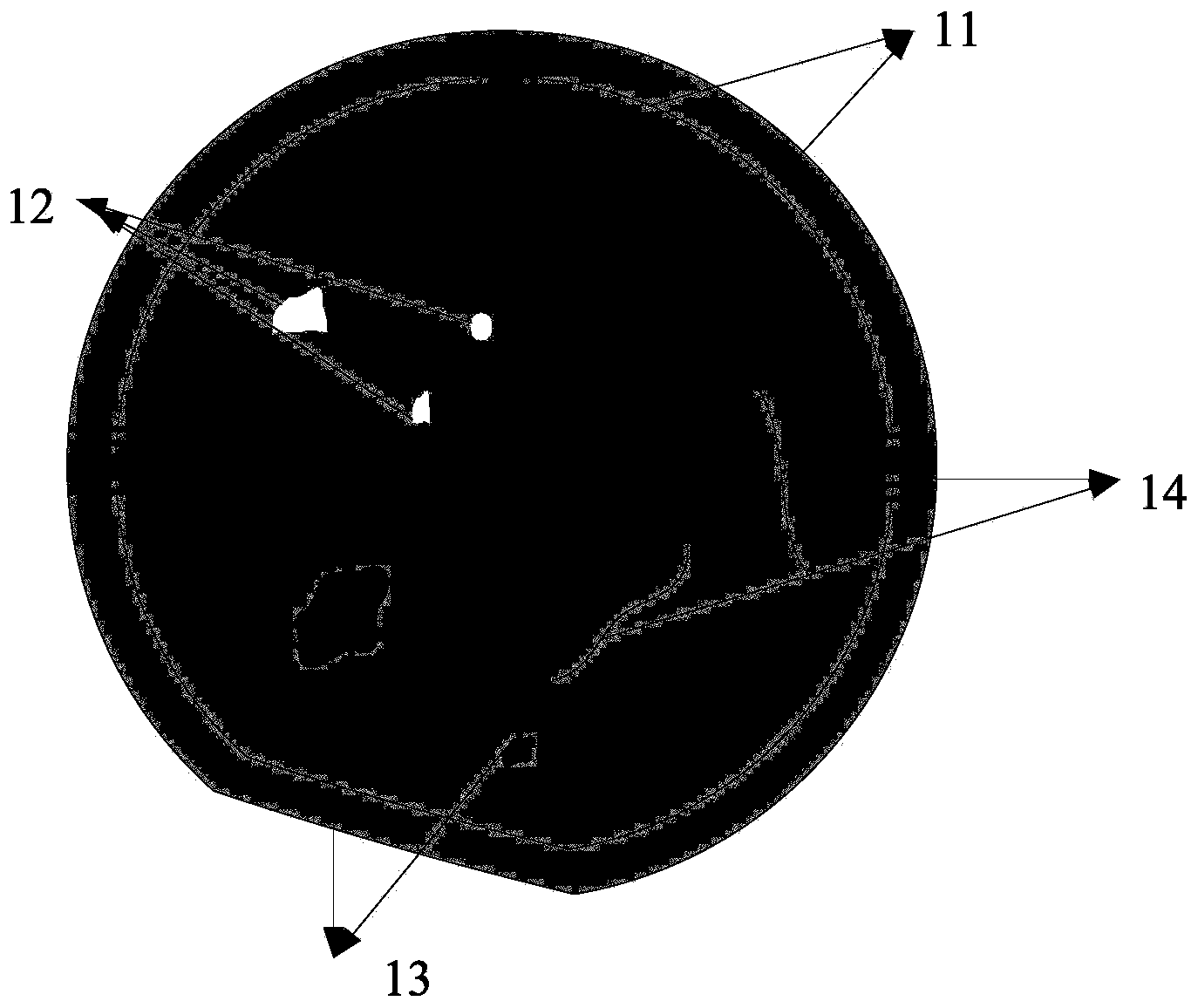
[0027] Such as figure 1 As shown, it is a schematic diagram of the main defects of the appearance of the wafer involved in the present invention. In this embodiment, the wafer is an LED-PSS wafer with a circular structure with cut edges. Among them, the number 11 is the edge of the wafer, and the outer edge is the outer edge, and the inner edge is the inner edge; the number 12 is a white defect; the number 13 is a black defect; and the number 14 is a scratch defect. White defects 12 may specifically include pinholes and image loss. Specifically, the black defect 13 may include large particle contamination and small particle contamination.

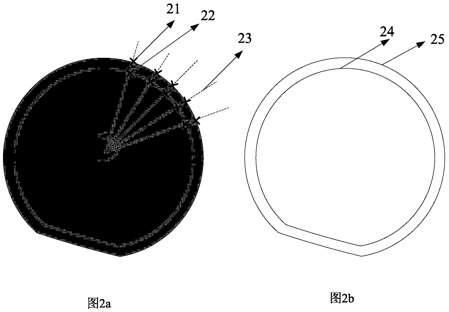
[0028] Such as Figure 2a with Figure 2b As shown, it is a schematic diagram of wafer edge scanning and edge width extraction according to the present invention. in, Figure 2a shows the edge sca...


PUM


Abstract

The invention relates to the field of semiconductor device manufacture equipment, and especially relates to a classification and detection method of wafer appearance defects. The method comprises the following steps: S1, screening to obtain a wafer image; S2, performing edge extraction on the wafer image to calculate the edge width; S3, segmenting out wafer region of interest; S4, performing appearance defect detection on the wafer region of interest; and S5, performing classification on wafer appearance defects. The method provided by the invention helps to improve the processing efficiency and quality of wafers.

Description

technical field [0001] The invention relates to semiconductor manufacturing technology, in particular to a method for detecting and classifying wafer appearance defects. Background technique [0002] Wafers are the basic material of semiconductors and the core part of LEDs. The quality of the wafer seriously affects the main photoelectric parameters such as the wavelength, brightness, and forward voltage of the LED. The quality of individual grains into which the wafer is cut affects the quality of semiconductor processing and also affects the efficiency of processing. Affecting the quality of semiconductor processing is mainly reflected in the pass rate of the product. If the quality of the grain is poor, the pass rate of the product will decrease. The impact on the processing efficiency is mainly reflected in the cutting of the defective part of the wafer, which will greatly reduce the processing efficiency. If judged by the data of the appearance inspection, the process...

Claims


Application Information

Patent Timeline
IPC IPC(8): G01N21/88
Inventor 舒远王光能周蕾米野高云峰
Owner HANS LASER TECH IND GRP CO LTD
Why Eureka
Try Eureka