Structuring of OLEDs using stack modification layer comprising perfluorinated vacuum grease and/or perfluorinated vacuum pump oil

a technology of perfluorinated vacuum grease and perfluorinated vacuum pump oil, which is applied in the direction of organic semiconductor devices, discharge tube luminescnet screens, and testing/measurement of semiconductor/solid-state devices, etc. it can solve the problems of large number of masks, limited shielded areas, and inability to fully cover the deposited material. , to achieve the effect of convenient, flexible and reliabl

Active Publication Date: 2015-11-24
KONINKLJIJKE PHILIPS NV
View PDF11 Cites 3 Cited by
  • Summary
  • Abstract
  • Description
  • Claims
  • Application Information

AI Technical Summary

Benefits of technology

[0006]It is an object of the invention to provide an easy, flexible and reliable method enabling a maskless structuring of the functional layer stack of OLED to provide OLEDs comprising non-emitting areas within the light-emitting area of the OLEDs while maintaining the same deposition processes for the functional layer stack as applied during mask processing.

Problems solved by technology

One major disadvantage of shadow masks is the need of one mask for each different pattern of masked areas resulting in a large number of required masks for manufacturing OLEDs with a varying pattern of non-emitting areas.
This large number of masks makes the mask process very expensive.
Another disadvantage of utilizing shadow masks is the limitation to shielded areas, which cannot be fully enclosed by deposited material.
This technique is limited to organic polymers, which is not the preferred light emitting material for OLEDs.

Method used


Image

  • Structuring of OLEDs using stack modification layer comprising perfluorinated vacuum grease and/or perfluorinated vacuum pump oil
  • Structuring of OLEDs using stack modification layer comprising perfluorinated vacuum grease and/or perfluorinated vacuum pump oil
  • Structuring of OLEDs using stack modification layer comprising perfluorinated vacuum grease and/or perfluorinated vacuum pump oil

Examples


example 1

Substrate Glass with ITO 150 nm on Top

[0046]Stack modification layer: Tyreno fluid (vacuum pump oil) applied manually with a paint-brush.

[0047]Organic layer stack: deposition of hole injector, hole transport layer, emitter layer, hole blocking layer and electron transport layer on top of substrate. Then LiF and Aluminum evaporated, common evaporation process.

[0048]Second electrode: Aluminum covers the second areas but does not attach to this film when there is a stack modification layer underneath as present within the first areas. Removal step: with FC-43 (washing) as the solvent, removes all visible traces of oil Cleaning step: Additional O2 plasma cleaning (see below)

example 2

Stack Modification Layer: TEC Grease

[0049]Removal step: with FC-43 as the solvent, washing with FC-43 dissolved the oil or the grease and allows removing the parts of the organic layers on top of the stack modification layer.

[0050]Cleaning step: O2 plasma cleaning (Diener electronics plasma processor “Nano”) removes last traces of stack modification layer or solvent. Cover lids can be applied by glue.

[0051]The not mentioned layers are the same as listed in example 1.

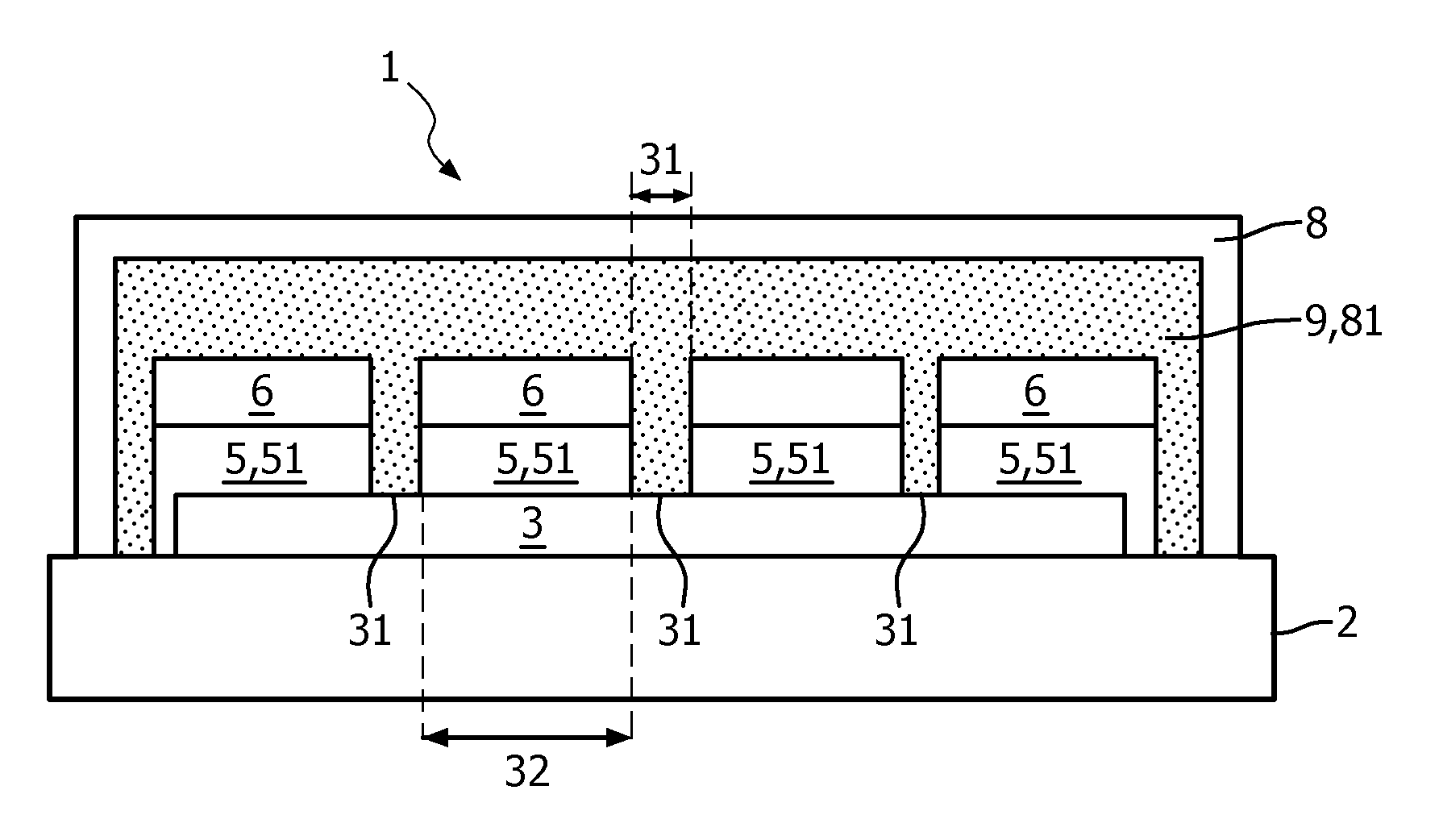
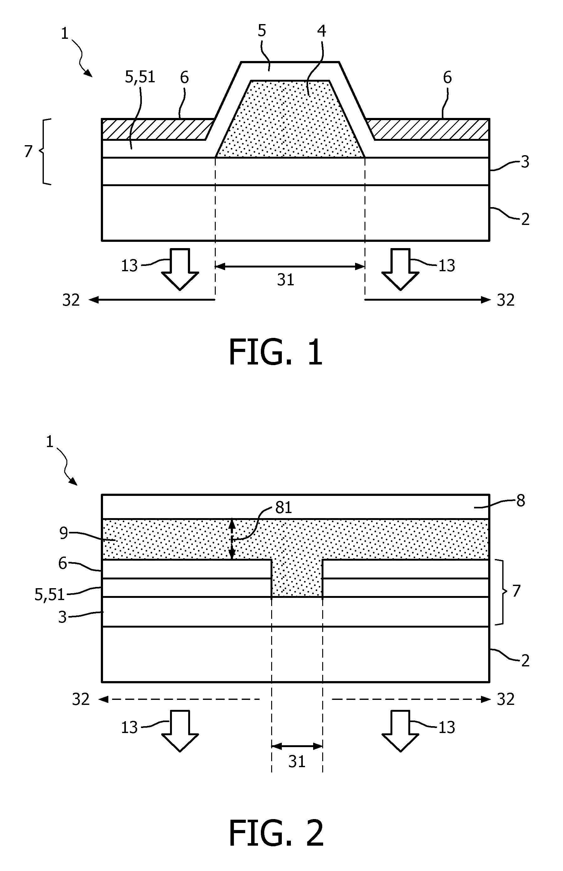
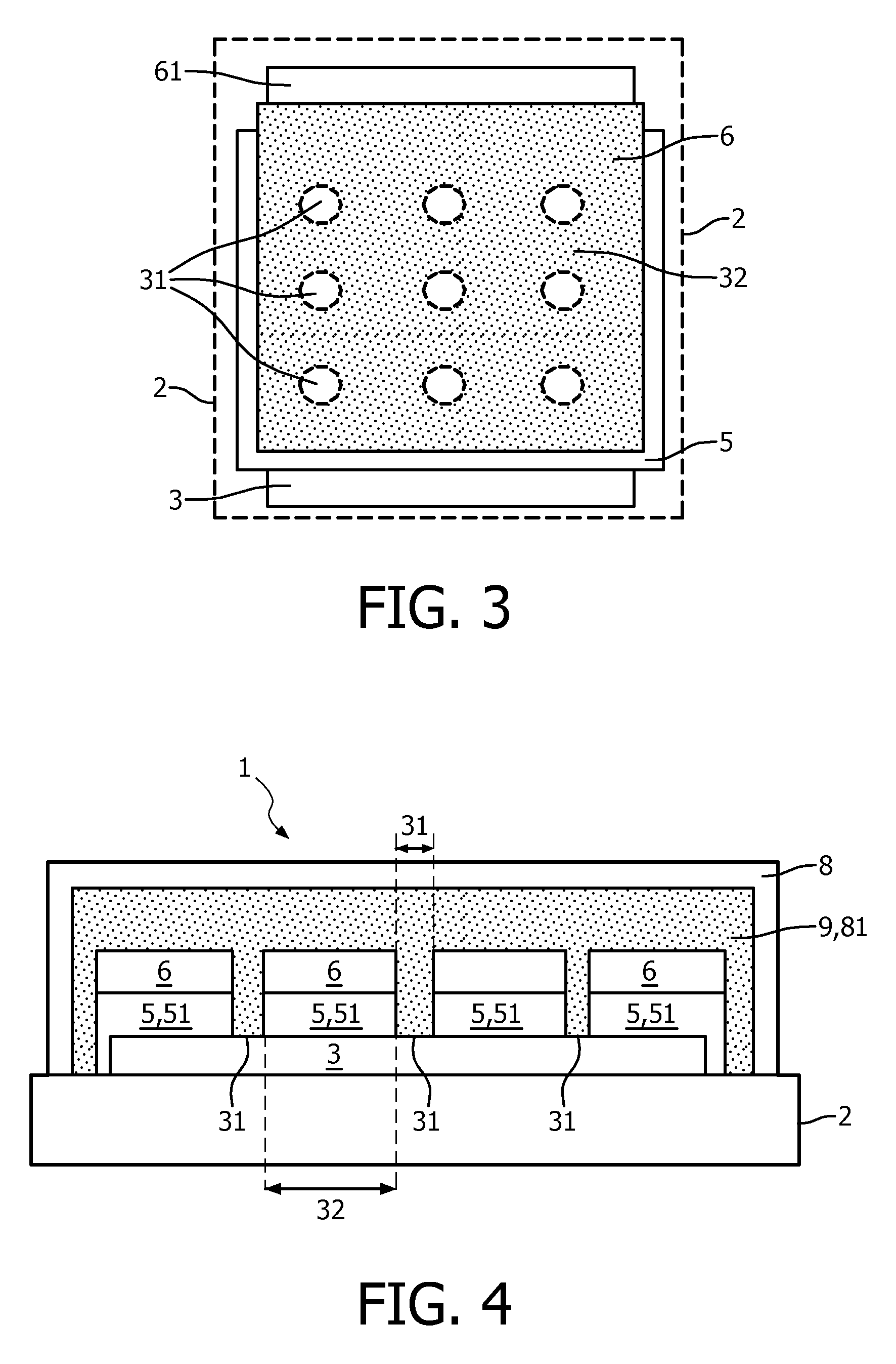
[0052]FIG. 6 shows one embodiment of the method steps for manufacturing OLED devices 1 according to the present invention out of an array of second areas 32 by cutting CT the substrate 2 along the first areas 31 (as indicated by the dashed lines CT). The second areas 32 are arranged in an array of rectangular shaped second areas 32 arranged in rows and columns with stripe like first areas 31 in between. The structured pattern are designed to separate light-emitting second areas 32 from each other by arranging first areas...


PUM


Abstract

The invention relates to a method for manufacturing structured organic electroluminescent light-emitting devices (OLEDs) comprising light-emitting and non-emitting areas and to OLEDs manufactured according to this method comprising the steps of: Providing (P) a substrate (2) covered at least locally with at least one conductive layer as the first electrode (3); Depositing (D-SML) a stack modification layer (4) locally on top of the first electrode (3) to establish first areas (31) covered with the stack modification layer (4) and non-covered second areas (32) adjacent to the first areas (31) forming the desired structured pattern; —Depositing (D-OLS) the organic layer stack (5) comprising at least one organic light-emitting layer (51) on top of the first electrode (3) locally coated with the stack modification layer (4) providing an organic layer stack (5) being separated from the first electrode (3) by the stack modification layer (4) in between the organic layer stack (5) and the first electrode (3) in the first areas (31) and being in direct electrical contract to the first electrode (3) in the second areas (32); and Depositing (D-SE) a conductive metal layer as the second electrode (6) on top of the organic layer stack (5) to finish a functional layer stack (7), wherein the first areas (31) above the stack modification layer (4) remain free of the conductive metal without masking these first areas (31); —Providing an easy, variable and reliable method of a maskless structuring of the functional layer stack of OLED enabling to maintain the same the same deposition processes for the functional layer stack as applied during mask processing.

Description

CROSS-REFERENCE TO PRIOR APPLICATIONS[0001]This application is the U.S. National Phase application under 35 U.S.C. §371 of International Application No. PCT / IB2012 / 055853, filed on Oct. 24, 2012, which claims the benefit of U.S. Provisional Patent Application No. 61 / 555,019, filed on Nov. 3, 2011. These applications are hereby incorporated by reference herein.FIELD OF THE INVENTION[0002]The invention relates to a method for manufacturing structured organic electroluminescent light-emitting devices (OLEDs) comprising light-emitting and non-emitting areas and to OLEDs manufactured according to this method.BACKGROUND OF THE INVENTION[0003]Standard OLEDs nowadays comprise an organic layer stack with at least one organic light-emitting layer arranged between two electrodes deposited on top of a substrate, typically a glass substrate, applying thin film deposition techniques. The layers between the two electrodes and the electrodes form an organic layer stack of thin layers with thickness...

Claims


Application Information

Patent Timeline
Patent Type & Authority Patents(United States)
IPC IPC(8): H01L29/08H01L21/66H01L51/40H01J1/62H01J63/04H01L51/56H01L51/52H01L35/24H01L51/00H01L27/32
CPCH01L51/56H01L27/3241H01L27/3283H01L51/5203H01L51/524H01L27/3281H01L2251/566H10K59/10H10K59/17H10K59/173H10K50/805H10K50/841H10K71/851H10K71/00H10K59/00
Inventor BOERNER, HERBERT FRIEDRICHHUMMEL, HELGA
Owner KONINKLJIJKE PHILIPS NV
Why Eureka
Try Eureka