Exposure device and exposure method

a technology of exposure device and exposure method, which is applied in the direction of microlithography exposure apparatus, photomechanical treatment, instruments, etc., can solve the problems of difficult control and match the position of the twin stages in the conventional exposure device, complex calibration process, and series of complex lithography processes. achieve the effect of improving accuracy and convenience in us

Active Publication Date: 2015-12-29
SEMICON MFG INT (SHANGHAI) CORP
View PDF16 Cites 1 Cited by
  • Summary
  • Abstract
  • Description
  • Claims
  • Application Information

AI Technical Summary

Benefits of technology

[0007]The present disclosure provides an exposure device and an exposure method using an accurately positioned stage to provide the exposure device with improved accuracy and conveniences in use.
[0010]As disclosed herein, clamp holders are configured on a stage. When a first substrate in a first clamp holder is exposed by an optical projection unit, the alignment mark of a second substrate is detected by a first or second alignment detection unit to align the second substrate. This improves production yield of the exposure device.
[0011]Further, the exposure device employs one stage and one measurement unit in which two optical interferometers (e.g., with one along x-axis direction and the other along y-axis direction), or three optical interferometers (e.g., with one along x-axis direction, one along y-axis direction, and one along z-axis direction) are involved. There is no need to employ two stages, two measurement units for the two stages, four optical interferometers (e.g., with two along x-axis direction and two along y-axis direction), or six optical interferometers (e.g., with two along x-axis direction, two along y-axis direction, and two along z-axis direction) as in conventional twin-stage exposure devices. The disclosed exposure device including, e.g., one stage and one measurement unit, avoids complex calibration and interferences among the interferometers. The stage can be more accurately positioned.
[0012]In addition, when the first substrate held by the first clamp holder is exposed by the optical projection unit, the second alignment detection unit detects an alignment mark of the second substrate held by the second clamp holder. When the second substrate held by the second clamp holder is exposed by the optical projection unit, the first alignment detection unit detects an alignment mark of the third substrate held by the first clamp holder. This can improve production yield of the exposure device.

Problems solved by technology

During semiconductor manufacturing processes, a series of complex and time-consuming lithography processes are performed mainly by corresponding exposure devices.
However, it is difficult to accurately control and match positions of the twin stages in conventional exposure devices.
In addition, conventional calibration processes are complex, which may affect accuracy (e.g., overlay accuracy) of the exposure devices and generate inconveniences in use.

Method used


Image

  • Exposure device and exposure method
  • Exposure device and exposure method
  • Exposure device and exposure method

Examples


Embodiment Construction

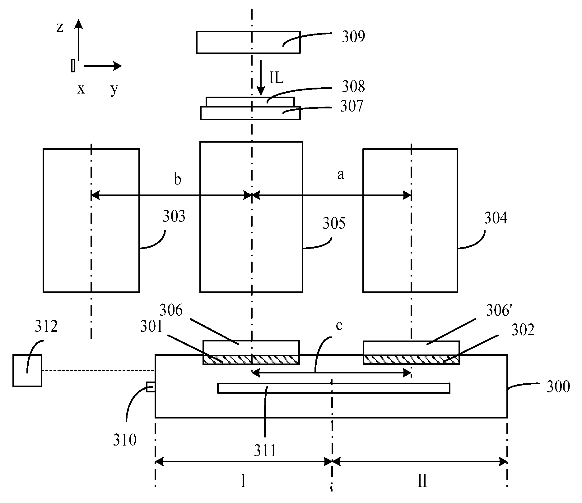
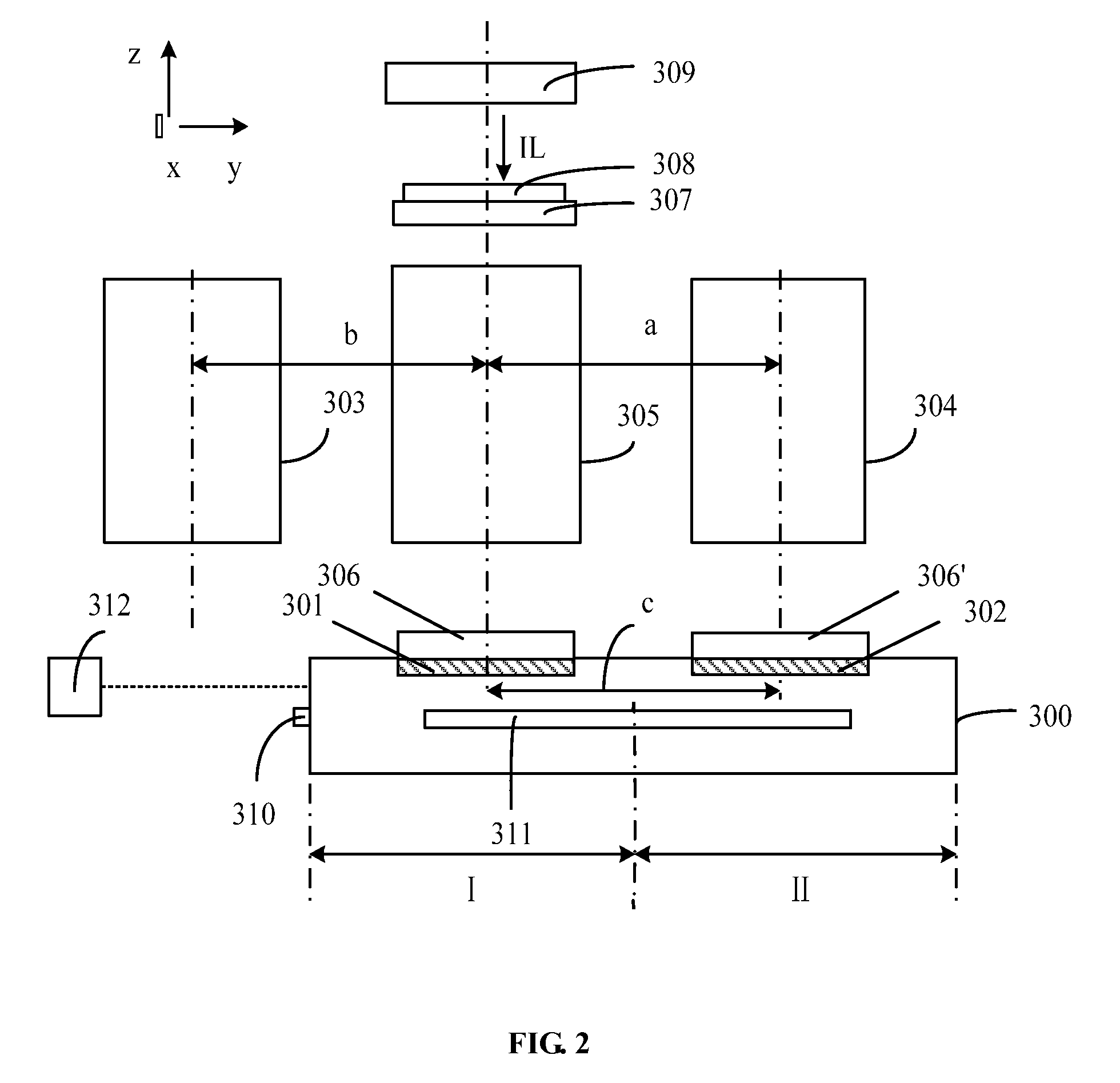
[0018]Reference will now be made in detail to exemplary embodiments of the disclosure, which are illustrated in the accompanying drawings. Wherever possible, the same reference numbers will be used throughout the drawings to refer to the same or like parts. For illustration purposes, elements illustrated in the accompanying drawings are not drawn to scale, which are not intended to limit the scope of the present disclosure. In practical operations, each element in the drawings has specific dimensions such as a length, a width, and a depth.

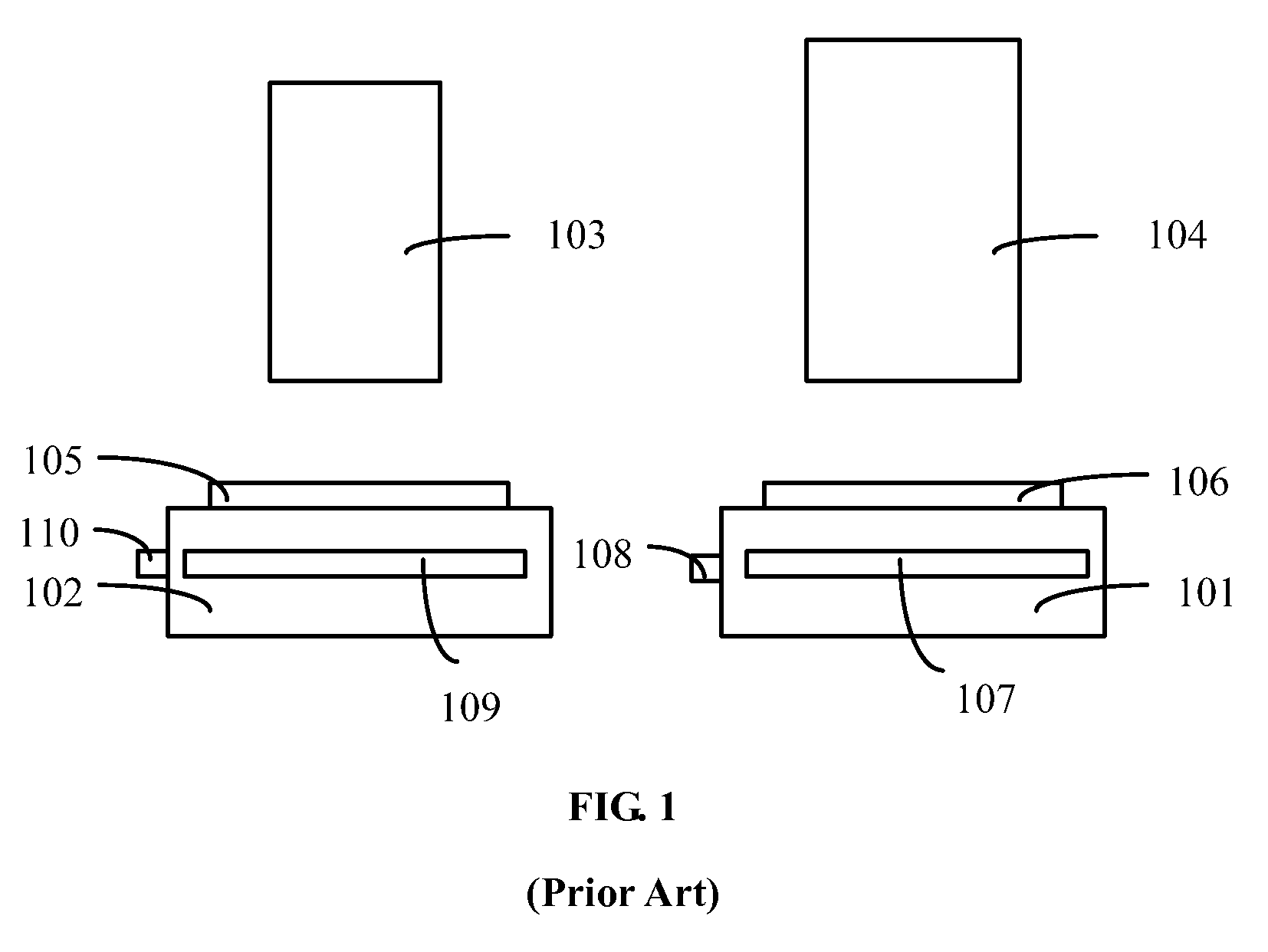
[0019]FIG. 1 is a schematic structural view of a conventional twin-stage exposure device. Referring to FIG. 1, the twin-stage exposure device includes: a first stage 101 and a second stage 102 for holding a substrate respectively; an alignment detection unit 103 for detecting alignment marks on the substrates; an optical projection unit 104 for exposing the substrates; and two measurement units (not shown) for measuring two dimensional coordinates ...


PUM

PropertyMeasurementUnit
wavelengthaaaaaaaaaa

Abstract

An exposure method and an exposure device are provided. An exemplary exposure device includes a stage, a first clamp holder, a second clamp holder, an optical projection unit, a first alignment detection unit, and / or a second alignment detection unit. The stage includes a first region and a second region. The first clamp holder is located in the first region and adapted for holding a first substrate, and the second clamp holder is located in the second region and adapted for holding a second substrate. The optical projection unit is located above the stage and adapted for exposure of the first substrate or the second substrate. The first alignment detection unit is adapted for detecting alignment marks of the first substrate. The second alignment detection unit is adapted for detecting alignment marks of the second substrate. The exposure device can accurately position the stage and improve production yield.

Description

CROSS REFERENCE TO RELATED APPLICATIONS[0001]The present application claims priority to Chinese Patent Application No. 201210028871.5, filed on Feb. 9, 2012, and entitled “Exposure Device and Exposure Method”, the entire disclosure of which is incorporated herein by reference.FIELD OF THE DISCLOSURE[0002]The present disclosure generally relates to the semiconductor manufacturing field and, more particularly, to an exposure device and an exposure method.BACKGROUND OF THE DISCLOSURE[0003]Lithography is considered as a key technique in semiconductor manufacturing processes, e.g., in manufacturing large scale integrated circuits (LSI). Lithography often includes a process for transferring patterns from a mask to a substrate by an exposure process. During semiconductor manufacturing processes, a series of complex and time-consuming lithography processes are performed mainly by corresponding exposure devices. Development of lithography technology or exposure devices has been made around t...

Claims


Application Information

Patent Timeline
Patent Type & Authority Patents(United States)
IPC IPC(8): G03F7/20G03F9/00
CPCG03F7/70725G03F7/70716G03F9/7003
Inventor WU, QIANGHAO, JING'ANLIU, CHANGYAO, XINLI, TIANHUISHU, QIANGGU, YIMING
Owner SEMICON MFG INT (SHANGHAI) CORP
Why Eureka
Try Eureka