

Method of manufacturing mask assembly for thin film deposition
a manufacturing method and technology of mask assembly, applied in the manufacture of tools, electroluminescent light sources, electric lighting sources, etc., can solve the problems of undesired separation between the division mask and the substrate, difficult to obtain high efficiency light emission, etc., to reduce or minimize the change of the division mask, reduce or minimize the interference between the welding points
- Summary
- Abstract
- Description
- Claims
- Application Information
AI Technical Summary
Benefits of technology
Problems solved by technology
Method used
Image

Examples
Embodiment Construction
[0027]It will be apparent to those skilled in the art that various modifications and variations can be made in the present invention without departing from the spirit or scope of the invention, and specific exemplary embodiments are exemplified in the drawings and explained in the detailed description. Thus, it is intended that the present invention covers modifications and variations of this invention provided they fall within the scope of the present invention and their equivalents.
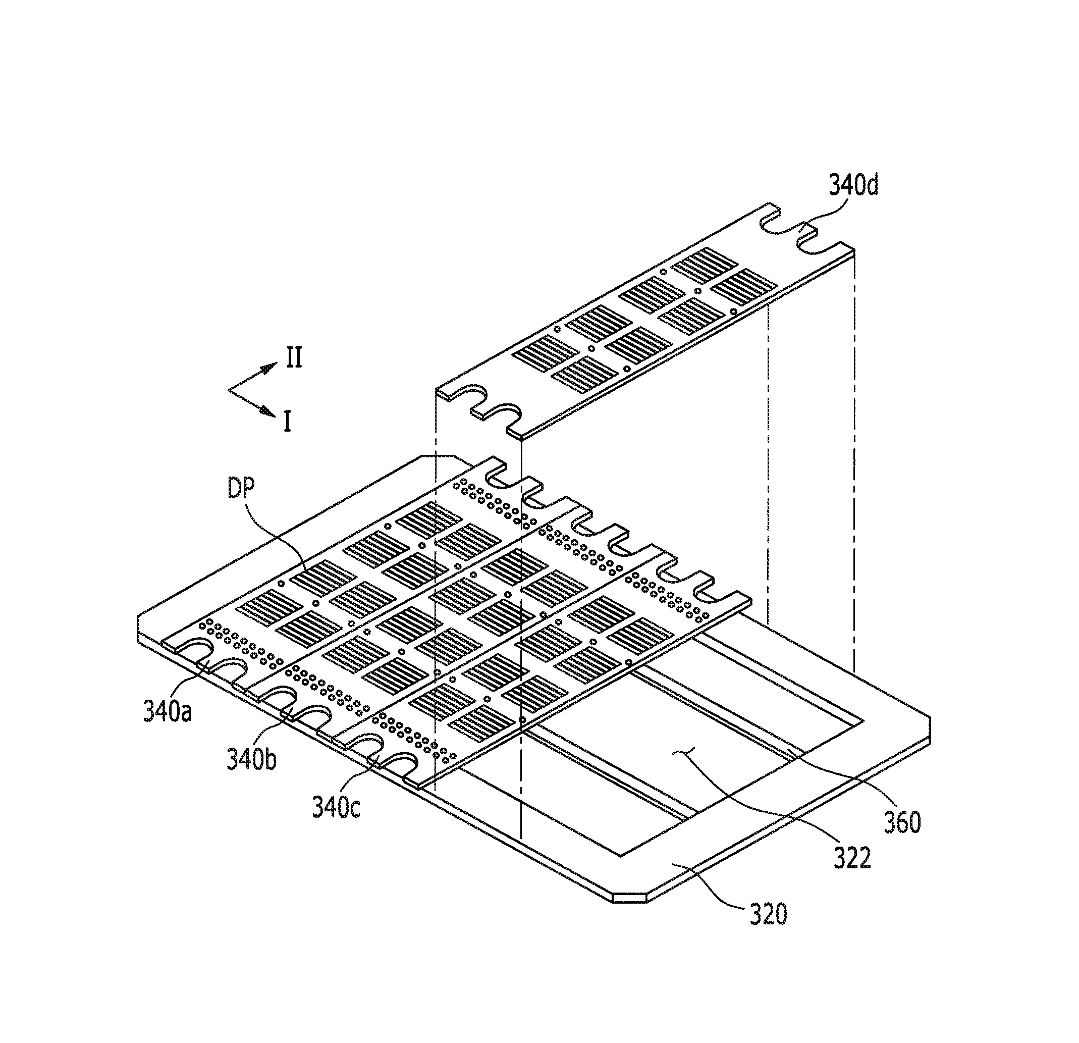
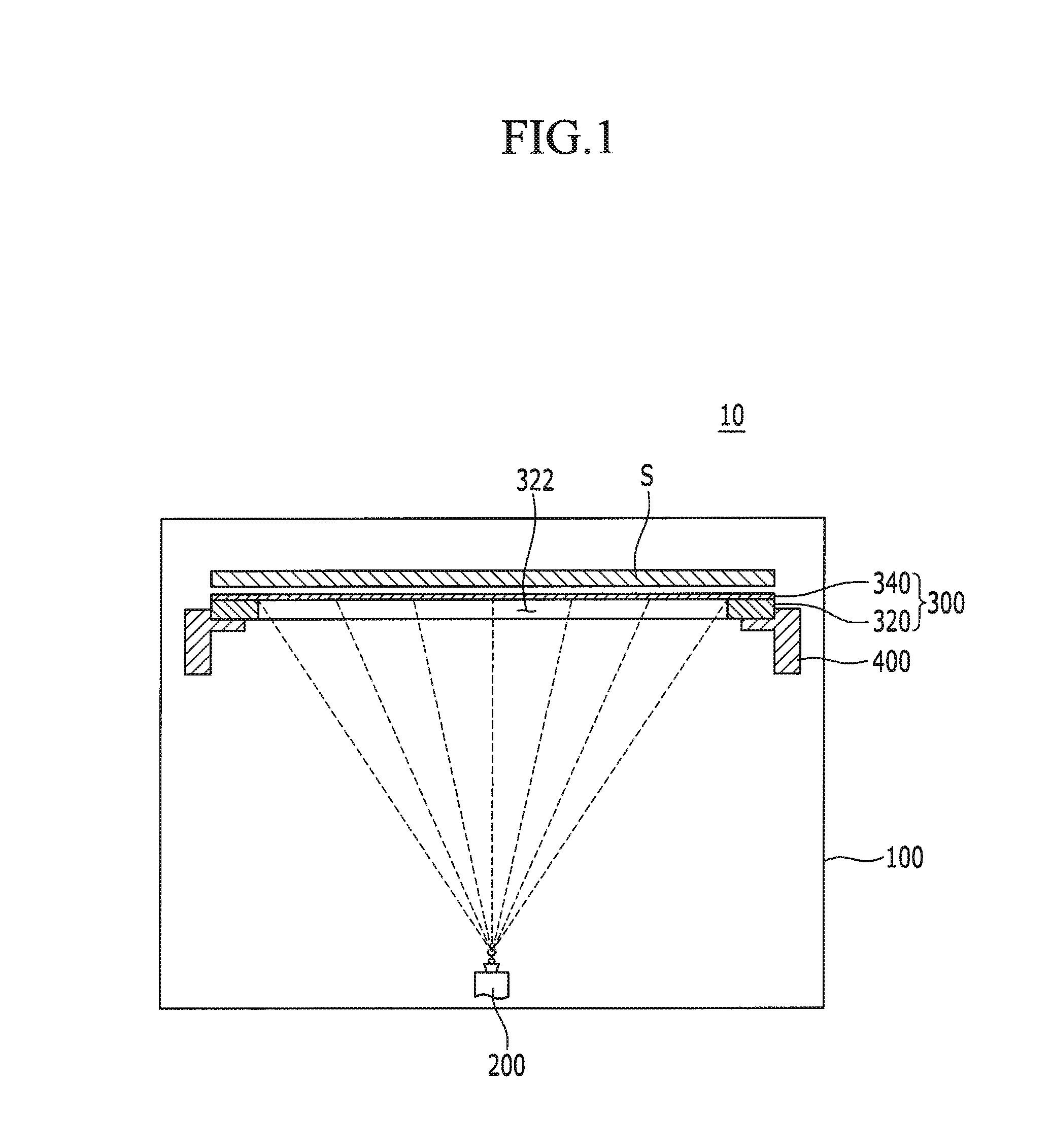
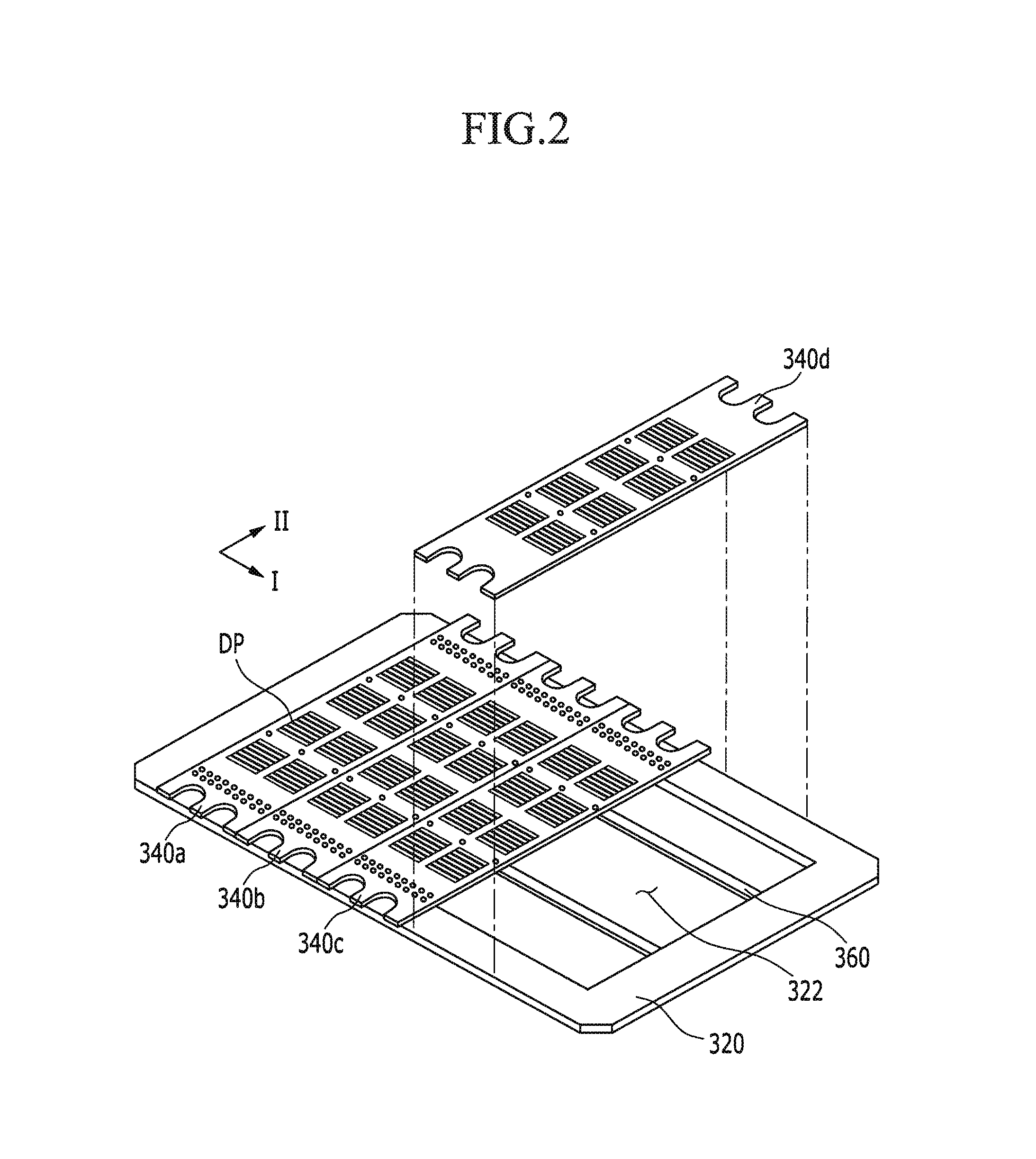
[0028]Like reference numerals designate like elements throughout the specification. In the drawings, the thickness of layers, films, panels, regions, etc., are exaggerated for clarity. The terms “first”, “second”, and the like may be simply used for description of various constituent elements, but the meanings may not be limited to restricted meanings. The above terms are used only for distinguishing one constituent element from other constituent elements. For example, a first constituent element may be...
PUM
| Property | Measurement | Unit |
|---|---|---|
| length | aaaaa | aaaaa |
| width | aaaaa | aaaaa |
| response speed | aaaaa | aaaaa |
Abstract
Description
Claims
Application Information