Method of forming fin-shaped structure

a technology of fins and structures, applied in the direction of basic electric elements, electrical apparatus, semiconductor devices, etc., can solve the problems of extreme challenge, physical limitations and various processing parameters, and achieve the effect of accurate layout of fins

Active Publication Date: 2016-02-16
UNITED MICROELECTRONICS CORP
View PDF40 Cites 21 Cited by
  • Summary
  • Abstract
  • Description
  • Claims
  • Application Information

AI Technical Summary

Benefits of technology

[0006]The present invention therefore provides a method of forming fin-shaped structures, which transfers the layout of spacers to a substrate to form fin-shaped structures, and then performs a cutting process to remove unnecessary parts of the fin-shaped structures. An accurate layout of fin-shaped structures can be achieved by this method, and uniform fin-shaped structures having the same widths in relative dense and isolate areas can be formed.

Problems solved by technology

Thus, forming fin-shaped structures which can achieve the required demands under the restrictions of miniaturization, physical limitations and various processing parameters becomes an extreme challenge.

Method used


Image

  • Method of forming fin-shaped structure
  • Method of forming fin-shaped structure
  • Method of forming fin-shaped structure

Examples


Embodiment Construction

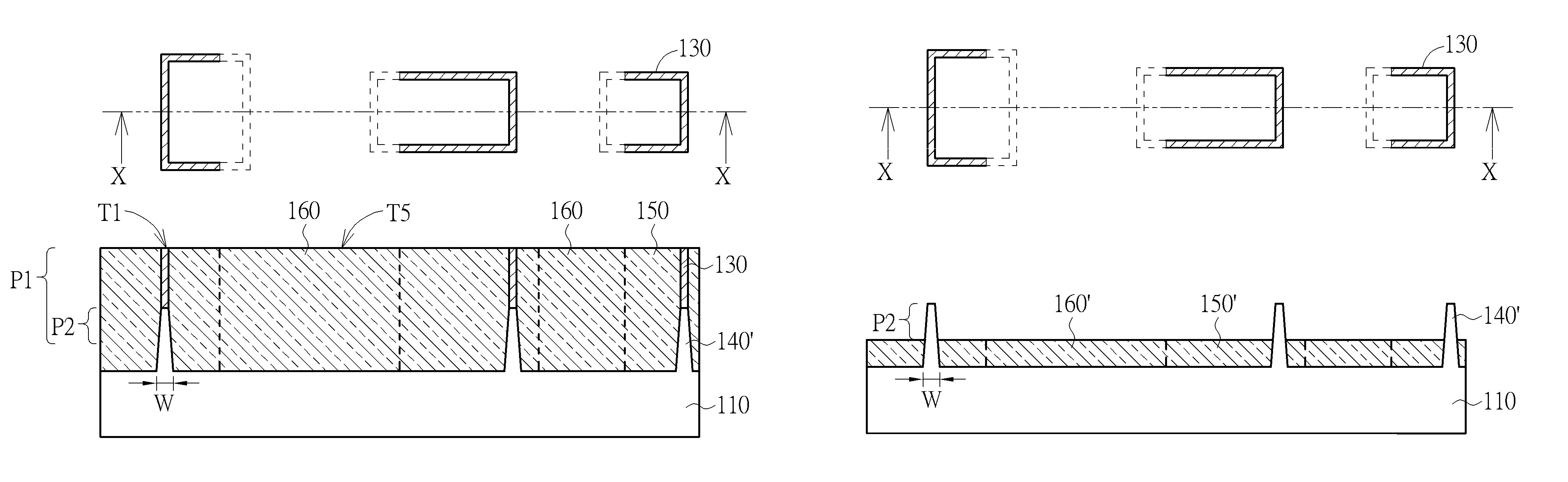
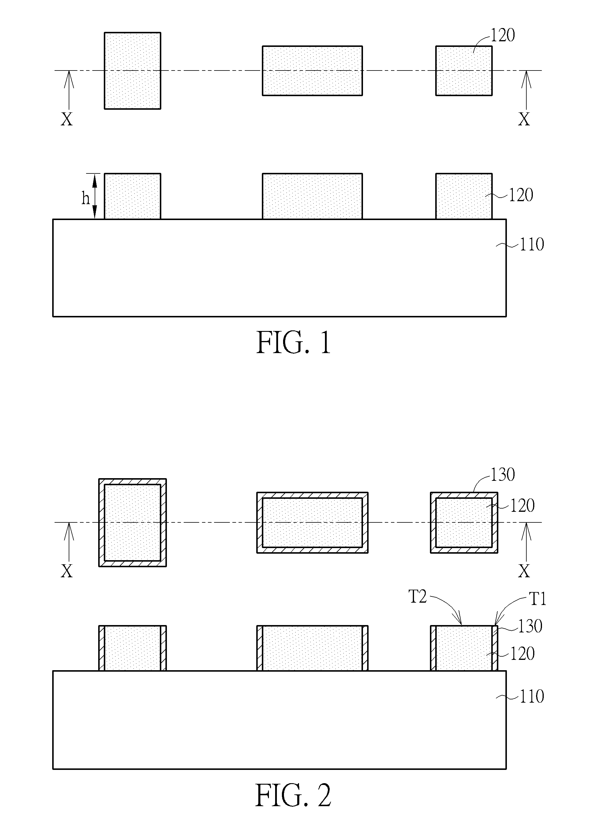
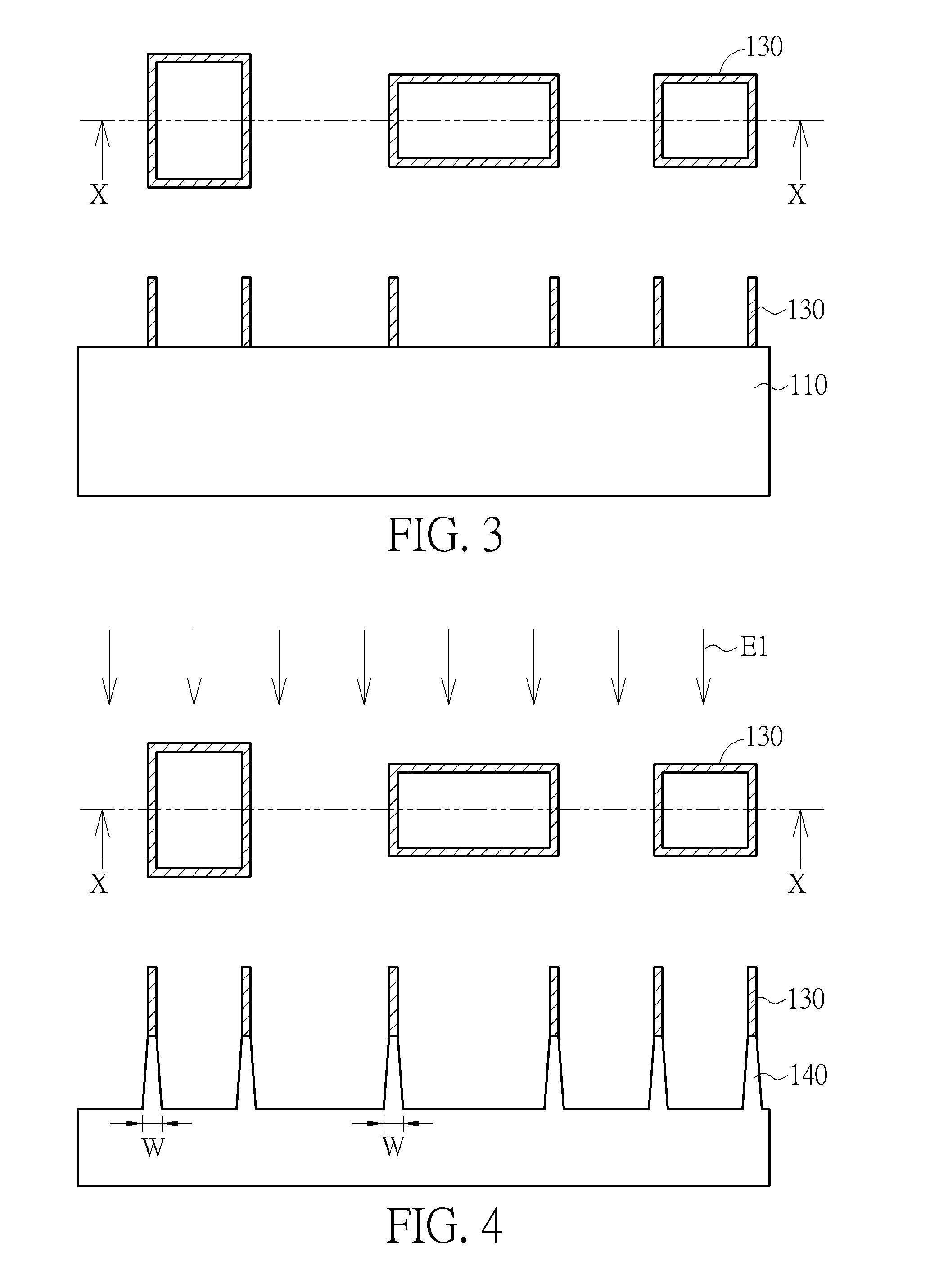
[0020]FIGS. 1-9 schematically depict cross-sectional views of a method of forming fin-shaped structures and a layout of spacers according to an embodiment of the present invention. Please refer to FIGS. 1-9, wherein the top diagrams of these respective figures depict top views of layouts of spacers, and the bottom diagrams of these respective figures depict cross-sectional views along direction X of top views of layouts of spacers.

[0021]As shown in FIGS. 1-3, a plurality of spacers 130 is formed on a substrate 110. More precisely, as shown in FIG. 1, a substrate 110 is provided. The substrate 110 may be a semiconductor substrate such as a silicon substrate, a silicon containing substrate, a III-V group-on-silicon (such as GaN-on-silicon) substrate, a graphene-on-silicon substrate or a silicon-on-insulator (SOI) substrate. A plurality of sacrificial patterns 120 are formed on the substrate 110. In this embodiment, the method of forming the sacrificial patterns 120 is integrated into ...


PUM


Abstract

A method of forming fin-shaped structures includes the following steps. A plurality of spacers is formed on a substrate. The substrate is etched by using the spacers as hard masks to form a plurality of fin-shaped structures in the substrate. A cutting process is then performed to remove parts of the fin-shaped structures and the spacers formed on the removed parts.

Description

BACKGROUND OF THE INVENTION[0001]1. Field of the Invention[0002]The present invention relates generally to a method of forming a fin-shaped structure, and more specifically to a method of forming a fin-shaped structure by transferring the pattern of spacers.[0003]2. Description of the Prior Art[0004]With increasing miniaturization of semiconductor devices, various Multi-gate MOSFET devices have been developed. The Multi-gate MOSFET is advantageous for the following reasons. Manufacturing processes of Multi-gate MOSFET devices can be integrated into traditional logic device processes, and thus are more compatible. In addition, since the three-dimensional structure of the Multi-gate MOSFET increases the overlapping area between the gate and the substrate, the channel region is controlled more effectively. This reduces both the drain-induced barrier lowering (DIBL) effect and the short channel effect. Moreover, as the channel region is longer for the same gate length, the current betwe...

Claims


Application Information

Patent Timeline
Patent Type & Authority Patents(United States)
IPC IPC(8): H01L21/302H01L21/308H01L29/66
CPCH01L21/3086H01L29/66795H01L21/76224
Inventor TSAO, PO-CHAOLIN, CHIEN-TING
Owner UNITED MICROELECTRONICS CORP
Why Eureka
Try Eureka